Wirebound inductor
Printed From: PCB Libraries Forum
Category: Libraries
Forum Name: Footprints / Land Patterns
Forum Description: [General or a CAD specific issues / discussions]
URL: https://www.PCBLibraries.com/forum/forum_posts.asp?TID=2837
Printed Date: 26 Jun 2026 at 1:12am
Topic: Wirebound inductor
Posted By: dramos
Subject: Wirebound inductor
Date Posted: 03 Mar 2021 at 5:55am
|
Hi to all: I am trying to create a footprint of a wirebound inductor, Murata LQW18AN5N6G80D. I configured my component as an SMD/Chip/Inductor and as the metalization of the pin part is not the height of the component, I configured the height of the part as the height of the metalization. 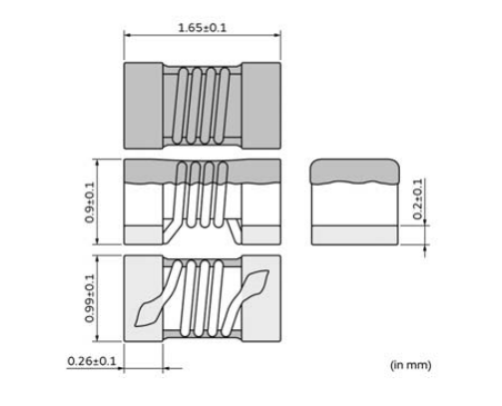 How do you resolve that kind of components? Thanks for your comments. dramos |
Replies:
Posted By: Tom H
Date Posted: 03 Mar 2021 at 9:53am
|
These Inductors are becoming more popular these days. There should be a mfr. recommended pattern for the footprint. If not, the pad size is: Heel = 0.00 but you need to compensate for the +/- body length tolerance of 0.10 Side = 50% of the metal thickness height up the side (Maximum) Toe = 100% of the metal thickness height up the side (Maximum) So the pad size for this part is 0.56 L X 1.20 W. Add 0.05 for the Heel to compensate for the tolerance. Here's a SolidWorks 3D model:  ------------- Stay connected - follow us! https://twitter.com/PCBLibraries" rel="nofollow - X - http://www.linkedin.com/company/pcb-libraries-inc-/" rel="nofollow - LinkedIn |
Posted By: dramos
Date Posted: 04 Mar 2021 at 12:17am
|
Hi Tom: Yes you are right . We are using more and more this kind of components in our designs. Many thanks for your recommendations. Regards. David
|
Posted By: IMI4tth3w
Date Posted: 04 Mar 2021 at 8:53am
|
I actually just did a footprint for one of these types of inductors. Coilcraft seems to have pretty good guidelines for footprints in their datasheets. Here's an example: https://www.coilcraft.com/en-us/products/rf/ferrite-core-chip-inductors/0603-" rel="nofollow - https://www.coilcraft.com/en-us/products/rf/ferrite-core-chip-inductors/0603- (1608)/0603ls/ https://www.coilcraft.com/getmedia/50061a32-b9f8-4dc5-bb10-57c731e20d9c/0603ls.pdf" rel="nofollow - https://www.coilcraft.com/getmedia/50061a32-b9f8-4dc5-bb10-57c731e20d9c/0603ls.pdf |
Posted By: Tom H
Date Posted: 04 Mar 2021 at 9:06am
|
Continue to use the mfr. recommended pattern for this new package style and new terminal lead form. Automating a software program to calculate the pad stack would need to identify a new terminal lead form and then the solder joint goal table for a 3-Tier density level. It's too late to put it in IPC-7351C and it's not in IPC-J-STD-001 yet for assembly solder joint acceptability. ------------- Stay connected - follow us! https://twitter.com/PCBLibraries" rel="nofollow - X - http://www.linkedin.com/company/pcb-libraries-inc-/" rel="nofollow - LinkedIn |
Posted By: Jeromeli
Date Posted: 01 Apr 2022 at 5:55am
| I have encountered a similar problem recently, and I am trying to solve it |
Posted By: Tom H
Date Posted: 01 Apr 2022 at 10:46am
|
You must use the Manufacturer's Recommended Pattern. ------------- Stay connected - follow us! https://twitter.com/PCBLibraries" rel="nofollow - X - http://www.linkedin.com/company/pcb-libraries-inc-/" rel="nofollow - LinkedIn |
Posted By: pem3bg
Date Posted: 30 Jun 2025 at 6:36am
|
Hi all, I'm trying to create footprint for an inductor like on the next picture: 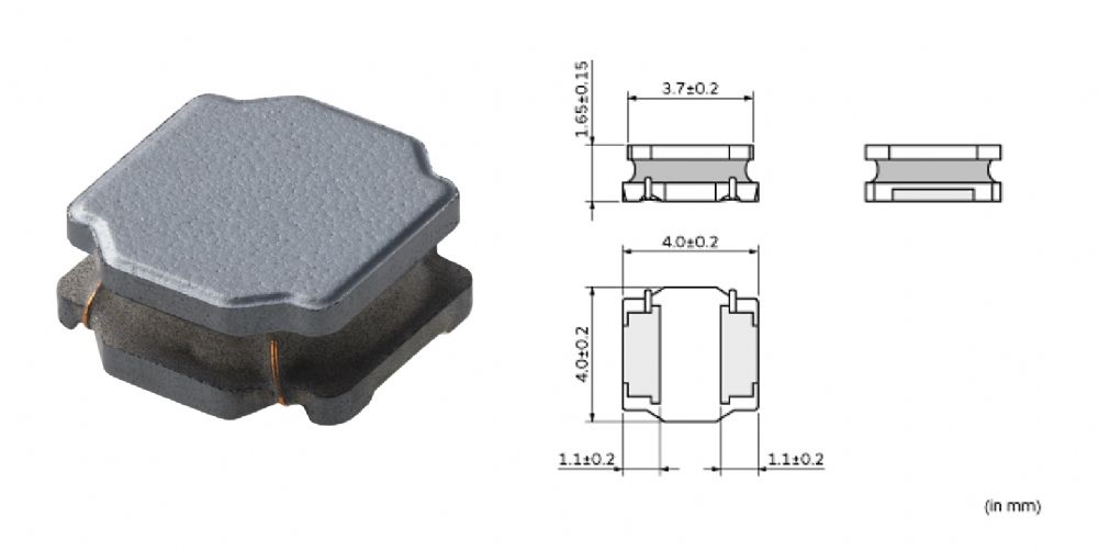
What would be the best type to use for this inductor (Chip Inductor or DFN 2 pins Inductor). I'm asking this because I want to have IPC name for this footprint and when I create footprint with both types I got different name. So what would be the best solution for this. It's Murata LQH44PN150MPRL |
Posted By: Tom H
Date Posted: 30 Jun 2025 at 7:36am
|
This Murata LQH44PN150MPRL have a trapezoid pad shape. It cannot be created in Footprint Expert, but we can build it in a CAD tool and export/import the ASCII file into FPX format. 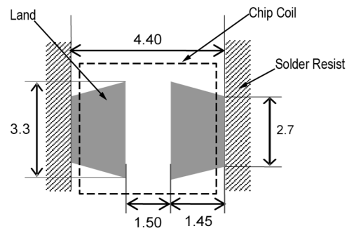 ------------- Stay connected - follow us! https://twitter.com/PCBLibraries" rel="nofollow - X - http://www.linkedin.com/company/pcb-libraries-inc-/" rel="nofollow - LinkedIn |