OrCAD 17.2: END LAYER Regular Pad Is Undefined
Printed From: PCB Libraries Forum
Category: PCB Footprint Expert
Forum Name: Questions & Answers
Forum Description: issues and technical support
URL: https://www.PCBLibraries.com/forum/forum_posts.asp?TID=2484
Printed Date: 26 Jun 2026 at 6:50pm
Topic: OrCAD 17.2: END LAYER Regular Pad Is Undefined
Posted By: shreyas.shroff
Subject: OrCAD 17.2: END LAYER Regular Pad Is Undefined
Date Posted: 14 May 2019 at 1:42am
|
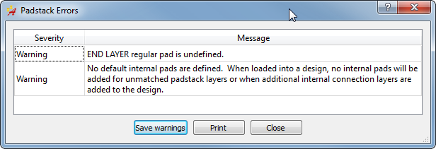
We recently updated our OrCAD PCB-Editor to 17.2. Now LE cannot build TH footprints anymore. The new Pad Stack Editor always throws up this warning:
 This is the script that caused the error (just as an example, since all others behave the same way): # Allegro script # Generated by FPX Expert # name: s218h145 QtSignal MainWindow New triggered QtSignal fileNewDialog dataCombo CurrentIndexChanged "Thru Pin" QtSignal fileNewDialog dataCombo activated "Thru Pin" QtSignal fileNewDialog browse clicked QtFillin s218h145.pad QtSignal fileNewDialog OK clicked QtSignal MainWindow Units CurrentIndexChanged Millimeter QtFillin Yes QtSignal MainWindow DecimalPlaces activated 4 QtSignal GuidedDrillTab HoleType activated Circle QtSignal GuidedDrillTab holeXSize editingFinished 1.45 QtSignal GuidedDesignLayersTab LayersTable cellClicked 0 "Regular Pad" None 0 2 QtSignal GuidedDesignLayersTab PadShape CurrentIndexChanged Square QtSignal GuidedDesignLayersTab PadShape activated Square QtSignal GuidedDesignLayersTab PadWidth editingFinished 2.18 QtSignal GuidedDesignLayersTab LayersTable cellClicked 1 "Regular Pad" None 1 2 QtSignal GuidedDesignLayersTab PadShape CurrentIndexChanged Circle QtSignal GuidedDesignLayersTab PadShape activated Circle QtSignal GuidedDesignLayersTab PadDiameter editingFinished 2.18 QtSignal GuidedDesignLayersTab LayersTable cellClicked 1 "Thermal Pad" None 1 3 QtSignal GuidedDesignLayersTab PadShape CurrentIndexChanged Circle QtSignal GuidedDesignLayersTab PadShape activated Circle QtSignal GuidedDesignLayersTab PadDiameter editingFinished 2.3 QtSignal GuidedDesignLayersTab LayersTable cellClicked 1 "Anti Pad" None 1 4 QtSignal GuidedDesignLayersTab PadShape CurrentIndexChanged Circle QtSignal GuidedDesignLayersTab PadShape activated Circle QtSignal GuidedDesignLayersTab PadDiameter editingFinished 2.3 QtSignal GuidedDesignLayersTab LayersTable cellClicked 2 "Regular Pad" None 2 2 QtSignal GuidedDesignLayersTab PadShape CurrentIndexChanged Square QtSignal GuidedDesignLayersTab PadShape activated Square QtSignal GuidedDesignLayersTab PadWidth editingFinished 2.18 QtSignal GuidedMaskLayersTab LayersTable cellClicked 0 Pad None 0 1 QtSignal GuidedMaskLayersTab PadShape CurrentIndexChanged Square QtSignal GuidedMaskLayersTab PadShape activated Square QtSignal GuidedMaskLayersTab PadWidth editingFinished 2.18 QtSignal GuidedMaskLayersTab LayersTable cellClicked 1 Pad None 1 1 QtSignal GuidedMaskLayersTab PadShape CurrentIndexChanged Square QtSignal GuidedMaskLayersTab PadShape activated Square QtSignal GuidedMaskLayersTab PadWidth editingFinished 2.18 QtSignal GuidedDrillSymbol FigureType CurrentIndexChanged Cross QtSignal GuidedDrillSymbol FigureType activated Cross QtSignal GuidedDrillSymbol FigureWidth editingFinished 1.0 QtSignal GuidedDrillSymbol FigureHeight editingFinished 1.0 QtSignal MainWindow Save triggered QtSignal MainWindow Exit triggered I have already checked the psmpath and psmpath settings and the both conatin the "." in the first place (although I don't think that this is the problem here, sinc SM Parts build correctly). I am running LE2016.10 Any ideas how to fix this? Regards Shreyas
 |
Replies:
Posted By: Tom H
Date Posted: 14 May 2019 at 8:30am
|
Did you read the OrCAD PCB import instructions in the User Guide? http://www.pcblibraries.com/products/fpx/userguide/default.asp?ch=205" rel="nofollow - http://www.pcblibraries.com/products/fpx/userguide/default.asp?ch=205 Did you select the OrCAD 17.2.048 translator? We can do a webcast with you to get you running again. ------------- Stay connected - follow us! https://twitter.com/PCBLibraries" rel="nofollow - X - http://www.linkedin.com/company/pcb-libraries-inc-/" rel="nofollow - LinkedIn |
Posted By: Tom H
Date Posted: 14 May 2019 at 8:36am
|
Suppress Drill Warnings. User Guide: http://www.pcblibraries.com/products/fpx/userguide/default.asp?ch=206" rel="nofollow - http://www.pcblibraries.com/products/fpx/userguide/default.asp?ch=206 Section 2.------------- Stay connected - follow us! https://twitter.com/PCBLibraries" rel="nofollow - X - http://www.linkedin.com/company/pcb-libraries-inc-/" rel="nofollow - LinkedIn |
Posted By: chrisa_pcb
Date Posted: 15 May 2019 at 8:28am
|
Make sure after you installed 17.2, that you fully patched up to S052, which is the current, I believe. You can check your patch level in Help -> About in either the Padstack Editor or OrCAD PCB Editor/Allegro. You should see an S (patch) level after the version callout. You will also need to make sure the version in our tool is selected as 17.2.048. If you don't see that, you need to patch our tool to current also. |