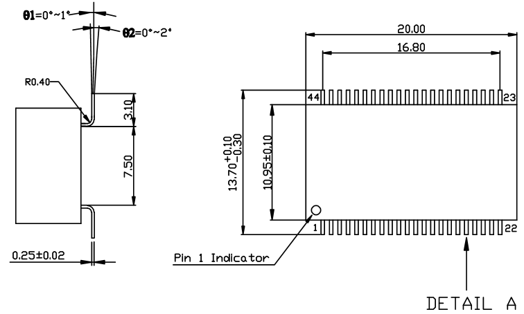
3D Plus Component
Printed From: PCB Libraries Forum
Category: PCB Footprint Expert
Forum Name: Questions & Answers
Forum Description: issues and technical support
URL: https://www.PCBLibraries.com/forum/forum_posts.asp?TID=1783
Printed Date: 22 Feb 2026 at 11:19am
Topic: 3D Plus Component
Posted By: AGONZ67
Subject: 3D Plus Component
Date Posted: 30 Oct 2015 at 5:32pm
|
Is there a correct package type in Library Expert to create an accurate landpattern for this component? SOL was the closest I could find but this is limited to 8 pins. uploads/71/package_w4.pdf" rel="nofollow - uploads/71/package_w4.pdf |
Replies:
Posted By: Tom H
Date Posted: 30 Oct 2015 at 9:20pm
|
This is a unique lead form that is not registered in any standard. It would require a mfr. recommended pattern. Or I would personally calculate the pad length and spacing using the math that is noted in "What's New in IPC-7351C" - http://www.pcblibraries.com/downloads/FPX!What-is-New-in-IPC-7351C.asp" rel="nofollow - download The "Pad Length" math calculation for a Nominal Density Level is (get the pad width and pad spacing from the IPC-7351C paper):
 ------------- Stay connected - follow us! https://twitter.com/PCBLibraries" rel="nofollow - X - http://www.linkedin.com/company/pcb-libraries-inc-/" rel="nofollow - LinkedIn |