Minimum Trace Width/Spacing for BGA
Printed From: PCB Libraries Forum
Category: General
Forum Name: General Discussion
Forum Description: general topics not related to other forums
URL: https://www.PCBLibraries.com/forum/forum_posts.asp?TID=1556
Printed Date: 26 Jun 2026 at 4:41am
Topic: Minimum Trace Width/Spacing for BGA
Posted By: SandroLanot
Subject: Minimum Trace Width/Spacing for BGA
Date Posted: 11 Feb 2015 at 3:03pm
|
Guys (& Gals), Can somebody please help advice what is the min trace width/spacing for 0.80 mm x 0.80 BGA? Thanks!
|
Replies:
Posted By: Tom H
Date Posted: 11 Feb 2015 at 3:12pm
|
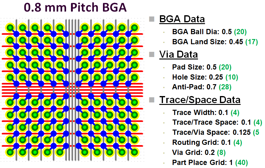
The numbers in Green are Mils.
------------- Stay connected - follow us! https://twitter.com/PCBLibraries" rel="nofollow - X - http://www.linkedin.com/company/pcb-libraries-inc-/" rel="nofollow - LinkedIn |
Posted By: SandroLanot
Date Posted: 11 Feb 2015 at 5:35pm
|
Thank you Tom, Actually, my plan is to use VIA18D9A26P (plugged from top open on bottom) if not near a pad on the bottom, and VIA18D9A26PTB plugged and cover with solder mask from both sides. |
Posted By: Tom H
Date Posted: 11 Feb 2015 at 7:46pm
|
Yes, I would highly recommend that you "Tent" the vias on the BGA side and leave the holes open on the bottom side. If you plug both sides, super heated gas in the hole could pop through the top or bottom solder mask but if you leave the bottom open it will let the heated gas during assembly reflow escape. If you want to cover both top and bottom holes I recommend that you fill the holes with something (over-plate, silver epoxy, solder mask) to eliminate the air in the hole. Super heated trapped air does things in assembly that damage the finished product. The last thing you need is popped air through solder mask under a BGA that you can't see. ------------- Stay connected - follow us! https://twitter.com/PCBLibraries" rel="nofollow - X - http://www.linkedin.com/company/pcb-libraries-inc-/" rel="nofollow - LinkedIn |