How To Specify Plated Holes?
Printed From: PCB Libraries Forum
Category: PCB Footprint Expert
Forum Name: Questions & Answers
Forum Description: issues and technical support
URL: https://www.PCBLibraries.com/forum/forum_posts.asp?TID=1400
Printed Date: 26 Jun 2026 at 9:00am
Topic: How To Specify Plated Holes?
Posted By: Aerolink
Subject: How To Specify Plated Holes?
Date Posted: 28 Aug 2014 at 8:52am
|
How do I specify that my pin holes are to be plated? I see there is a checkbox that say's "Plated" when I view the pad stack. The box is checked and greyed-out but my boards came back with unplated holes. Did I miss something? |
Replies:
Posted By: Tom H
Date Posted: 28 Aug 2014 at 9:06am
|
We need to know if you are referring to the IPC Calculator or FP Designer. We also need to know what version of Library Expert are you using? V2014.08 is the latest release with updates to the FP Designer Pad Stack Manager. ------------- Stay connected - follow us! https://twitter.com/PCBLibraries" rel="nofollow - X - http://www.linkedin.com/company/pcb-libraries-inc-/" rel="nofollow - LinkedIn |
Posted By: Aerolink
Date Posted: 29 Aug 2014 at 7:55am
|
V2013.20 FP Designer |
Posted By: Tom H
Date Posted: 29 Aug 2014 at 8:07am
|
You should download V2013.21. That will help. I haven't used V2013 since last February and FP Designer has a completely new Pad Stack Manager in the current V2014.08.
------------- Stay connected - follow us! https://twitter.com/PCBLibraries" rel="nofollow - X - http://www.linkedin.com/company/pcb-libraries-inc-/" rel="nofollow - LinkedIn |
Posted By: ernestorey
Date Posted: 29 Aug 2014 at 1:50pm
|
You should always review your GERBER files prior to sending them out, use an independent GERBER viewer (not tied to the layout tool) to check the outputs. I recommend ViewMate from http://www.pentalogix.com/" rel="nofollow - www.pentalogix.com , been using it for 10+ years.
Regarding your holes, if drilled through a metal pad they will be plated. If there is no metal on the outer layers they will be unplated. If the metal is the same size as the finished hole size, they will be unplated since they need to be drilled larger in order to plate.
On many drill data outputs the plated/not-plated information is not encoded in the NC files, you should have a drill "map" or "chart" as part of the GERBERs or the Fabrication Drawing specifying which holes you want plated or unplated.
|
Posted By: Aerolink
Date Posted: 31 Aug 2014 at 9:52am
|
Unfortunately, when using SoloPCB for layout, we are not given access to our Gerbers until after the board is purchased! This has caused a lot of trouble for me and after one round of bad boards I convinced my vendor (Mass Design) to share the files with me. I spotted that problem right away. Unfotunately, round two has this thru-hole plating problem. I need to figure this out before round three. BTW, I use the same viewer as you,,, when I have files to view. Anyway, back to the problem. On EVERY thru-hole component I have created, my actual boards come back without plated holes. Every hole that is to be connected to a power or ground plane is not connected due to lack of plating. The gerbers look correct. They show thermal reliefs to the pin hole when I view the plane layers. There are no top or bottom layer signals to these pins but the pad rings look normal and are plated, just not the bores. You may be onto the problem with the hole sizes versus drill sizes. I don't know the mfg process, but could they have drilled out the plating? All I find related to this is the greyed out, but checked, "Plated" checkbox on the padstack manager. Not sure why it is greyed out, but at least it is checked. The pad size is 2.20 and hole is 1.6, so I don't see a problem there. I just want to understand how this works from the library point of view to see if I missed something when I created these footprints. I will post to the SoloPCB forum too. I hate to think this is a problem with the PCB Library version I am using?!?! Certainly someone else would have run across this by now? |
Posted By: Aerolink
Date Posted: 31 Aug 2014 at 9:55am
|
Is there any reason why I shouldn't just upgrade to 2014-08? You suggested a 2013 version. |
Posted By: Tom H
Date Posted: 31 Aug 2014 at 10:07am
|
You should upgrade to V2014.09 which will be available next week -
------------- Stay connected - follow us! https://twitter.com/PCBLibraries" rel="nofollow - X - http://www.linkedin.com/company/pcb-libraries-inc-/" rel="nofollow - LinkedIn |
Posted By: Aerolink
Date Posted: 31 Aug 2014 at 11:44am
|
Will do... Does the footprint convey plated versus non-plated holes to the layout tools or not? As I look into this further, I find nothing in the footprint that would indicate that holes are NOT to be plated. The "Plated" checkbox seems always to be checked, as I would expect for a thru-hole part. I just reviewed my drill layer in SoloPCB and sure nuf, the drill chart says "Non-Plated" for all of the holes related to my footprints. I can use the SoloPCB's padstack editor to mark these holes as plated (clearing the "Non-Plated" checkbox) and all looks well again.... So.... where did this fall apart? Does the footprint convey platedness to the layout tools? If so, then the layout tool is not honoring this info. If the footprint does NOT convey plated info, then it would appear to be human error (me of course) for not knowing enough to edit the padstacks that need plating (seems like a sensible "default" for thru-hole parts to me). |
Posted By: Tom H
Date Posted: 31 Aug 2014 at 12:52pm
|
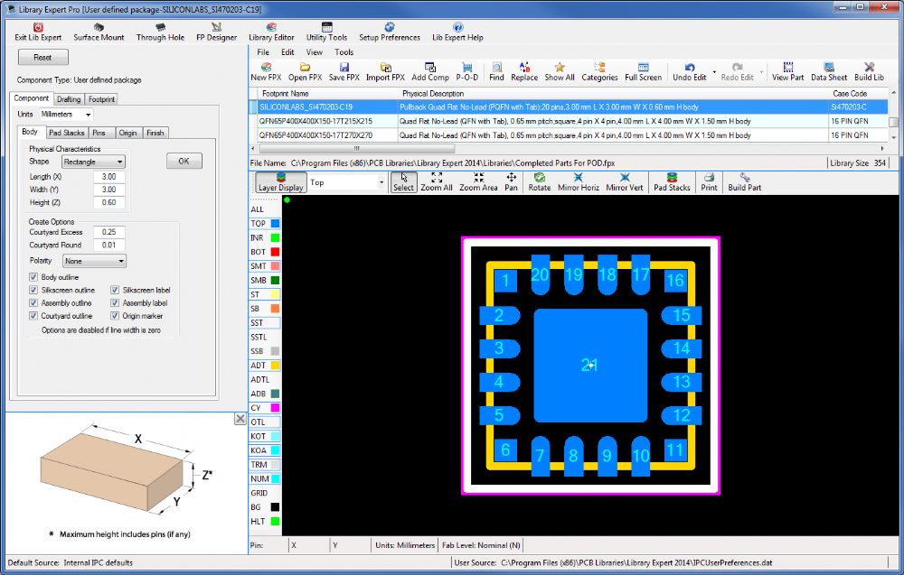
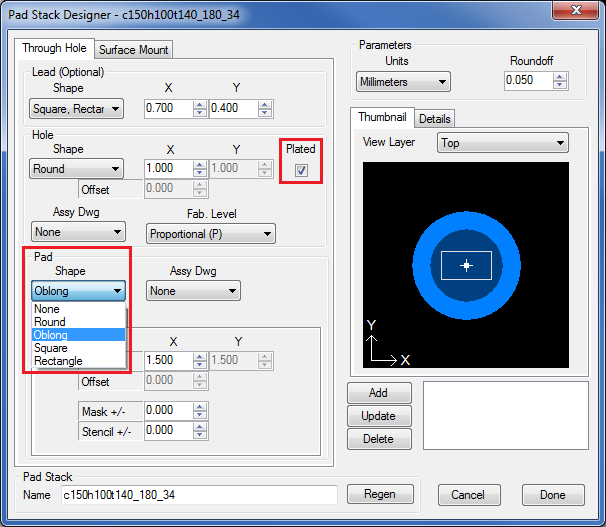
In the through-hole Calculator component families, every hole is automatically plated and you have no control of that with the exception of the Mounting Hole calculator can toggle Plated or Non-plated. The FP Designer the user has a Plated check box and an assortment of pad shapes. And even though the calculator will provide a good annular ring, the user can override the calculation and enter a unique pad size.
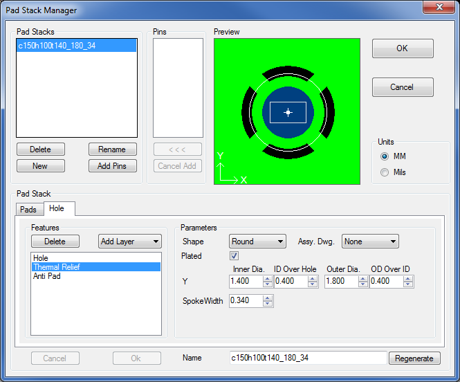
Once the pad stacks are created and you select the "Done" button, the Pad Stack Manager dialog window will open. That allows the user to further customize each pad stack for outer and inner layers, solder and paste mask, anti-pad and thermal relief, making the FP Designer totally flexible to create unique pad stacks.
------------- Stay connected - follow us! https://twitter.com/PCBLibraries" rel="nofollow - X - http://www.linkedin.com/company/pcb-libraries-inc-/" rel="nofollow - LinkedIn |
Posted By: Tom H
Date Posted: 04 Sep 2014 at 12:57pm
|
V2014.09 with this new technology will be released today. We will send out an email notification when it's ready for download. ------------- Stay connected - follow us! https://twitter.com/PCBLibraries" rel="nofollow - X - http://www.linkedin.com/company/pcb-libraries-inc-/" rel="nofollow - LinkedIn |
Posted By: Aerolink
Date Posted: 04 Sep 2014 at 1:09pm
|
Just to wrap up this thread, below is the reply I received from FabStream regarding this issue. I will try the new version, but since these boards are already finished and they utilized approx 60 footprints created by the older version, what do I need to do to propagate this fix into my designs? Presumably I have to "build" all of the affected parts again to update my library, but deleting and replacing the parts in my layout is a no-go since it would destroy a huge amount of manual routing. Should I build the parts as "alternate" footprints and select the alternates in SoloPCB? Seems like it might work, but this is round three for this board so I'd like to be sure. ...from FabStream... "We have confirmed with PCB Libraries that there was an error in their Library Pro Expert product. The error was discovered and corrected. A new 2014.09 release will be made available tomorrow (09-03-2014) that has the correction. The product incorrectly defined plated pads as non-plated in SoloPCB." "PCB Libraries also informed us the person that discovered the error (ALINK) is eligible for a free upgrade to their 2015 release. You should contact them directly for this upgrade." "The type of checking you suggest (detect opens that result from lack of plating in a hole) are not presently available in the SoloPCB product is planned for a future release." FabStream Support |
Posted By: Tom H
Date Posted: 04 Sep 2014 at 1:16pm
|
Once you download and install V2014.09, open your FPX file and select the upper left corner cell (next to the Footprint Name column header) to highlight your entire FPX file. Then select "Build Lib" button and regenerate your entire library. In your case, contact Nick Ban and he will upgrade your license to include V2015 and all the updates to it for the next year for free. Note: this issue was fixed in OrCAD Layout and SoloPCB. ------------- Stay connected - follow us! https://twitter.com/PCBLibraries" rel="nofollow - X - http://www.linkedin.com/company/pcb-libraries-inc-/" rel="nofollow - LinkedIn |
Posted By: ernestorey
Date Posted: 04 Sep 2014 at 2:10pm
| I personally would never use again a PCB fabricator who gets a design with all holes unplated and never flags this out to the customer. Do they do any preCAM inspection? |
Posted By: Tom H
Date Posted: 04 Sep 2014 at 2:15pm
|
I totally agree with you. If a PCB manufacturer gets fabrication data with no plated holes, that's a red flag, stop production and notify the PCB designer to make sure. I haven't heard of a non-plated through-hole board since the 1970's. ------------- Stay connected - follow us! https://twitter.com/PCBLibraries" rel="nofollow - X - http://www.linkedin.com/company/pcb-libraries-inc-/" rel="nofollow - LinkedIn |
Posted By: Aerolink
Date Posted: 05 Sep 2014 at 9:41am
|
You're right, I am not happy with my board vendor's (MassDesign) lack of understanding and involvement in this process, but I need "assembly" not just PCB's and they are one of the few supported vendors. The concept of FabStream's SoloCapture/SoloPCB tools is that the tools are "free" but you are locked into a board vendor because they do not provide the gerber files. I had to point out that MassDesign's own advertisement on the FabStream site says "Free CAD files" then pester them for days to get the files. But you still don't get them until AFTER ordering the boards, which means you lose the ability to review and resolve physical issues. Bad business model, IMHO. So I am in round-three of my prototype design (at $360 a pop) because of tool errors I could not have detected. The SoloPCB tools do not detect the plated hole issue (they say it will be done in the future) and MassDesign's response was "garbage in = garbage out". They do no electrical testing on boards coming in from this process. I have used MassDesign for years on other products, but not with this tool suite. They clearly treat these tools as hobbyist's toys. ...but in all fairness, the plating issue has turned out to be a problem with Library Expert PRO. The lack of detection and prior issue of starved, overlapping thermal reliefs, has turned out to be problems with FabStream's tools, and the further lack of detection and general don't care attitude, is from MassDesign. While we are spreading the blame around, I too am to blame for jumping onto a relatively unproven set of tools rather than sticking with what has worked for years. Fortunately, the cost of these multiple rounds of rework will be absorbed by profits down the road. Gotta spend money to make money! |
Posted By: Tom H
Date Posted: 05 Sep 2014 at 9:48am
|
I'm positive that Downstream will fix the problem of DRC checking for Non-plated holes. Every CAD vendor has regression and bugs and that's just everyday software programming. Having a bug is not the problem. How long it takes to fix the bug is a problem. We've had our share of regression in the past month by trying to implement too many new features too fast. V2014.09 has just been released 5 minutes ago that fixed a final bug that was reported last night. ------------- Stay connected - follow us! https://twitter.com/PCBLibraries" rel="nofollow - X - http://www.linkedin.com/company/pcb-libraries-inc-/" rel="nofollow - LinkedIn |