LED PLCC footprints
Printed From: PCB Libraries Forum
Category: Libraries
Forum Name: Footprints / Land Patterns
Forum Description: [General or a CAD specific issues / discussions]
URL: https://www.PCBLibraries.com/forum/forum_posts.asp?TID=1187
Printed Date: 26 Jun 2026 at 2:17am
Topic: LED PLCC footprints
Posted By: HenricE
Subject: LED PLCC footprints
Date Posted: 20 Nov 2013 at 6:30am
|
I've been wondering over the naming of certain LED footprints. Manufacturers call them PLCC-4, PLCC-6 etc etc. They have pins only on two sides and when compared to the typical PLCC footprints found in for example FPX they show pins on all four sides. Those particular PLCC footprints also appear to fit into sockets rather than directly soldered to the PCB. Looking through the FPX list of footprint types I suppose the Small Outline L-Lead fits better. Which one is correct and what should the footprint actually be named? Examples: http://www.avagotech.com/docs/AV02-2592EN" rel="nofollow - http://www.avagotech.com/docs/AV02-2592EN http://www.vishay.com/doc?81183" rel="nofollow - http://www.vishay.com/doc?81183 |
Replies:
Posted By: Tom H
Date Posted: 20 Nov 2013 at 7:09am
This Lead Form is "L-Bend" - (not PLCC)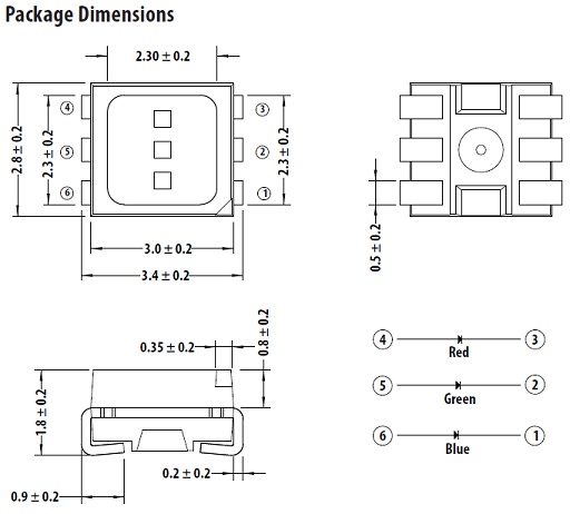 We just added a "L-Bend" component lead for IC's. It's called the SOL component family. Looks like we need to add a drop down to include other component families like LED. There is also a "L-Bend" lead for Oscillators. ------------- Stay connected - follow us! https://twitter.com/PCBLibraries" rel="nofollow - X - http://www.linkedin.com/company/pcb-libraries-inc-/" rel="nofollow - LinkedIn |
Posted By: HenricE
Date Posted: 20 Nov 2013 at 7:15am
|
Thanks for the quick reply! The SOL component family did look a lot more like the actual LEDs. It's strange how the manufacturers have chosen to call them PLCC. |