

|
|
New 2016 Solder Joint Goals |
Post Reply 
|
Page 12> |
| Author | |
Tom H 
Admin Group 

Joined: 05 Jan 2012 Location: San Diego, CA Status: Offline Points: 6075 |
 Post Options Post Options
") Thanks(0) Thanks(0)
 Quote Reply Quote Reply
 Topic: New 2016 Solder Joint Goals Topic: New 2016 Solder Joint GoalsPosted: 03 Jul 2016 at 2:12pm |
|
PCB Libraries, Inc. introduces new advanced solder joint goals for the IPC-7351 3-Tier library system. Following the IPC-J-STD-001 standard for solder joint acceptability for each Terminal Lead-form, our research team has determined that the IPC-7351B specifies unnecessarily long Toe goals for many of these component lead types.
Trimming the Toe also makes the courtyard excess smaller. The IPC-7351 standard has a “One Goal Fits all leads” philosophy and we have found that to have many faults. Example: the Gull Wing lead has the same exact solder joint goals for SOP, QFP, SOD, SOT and DPAK regardless of pin pitch, lead frame thickness, package pin quantity or package weight. Another example: IPC-7351B Concave and Rectangular End Cap (Chip) lead-forms each only have 2 options for Toe, Heel and Side solder joints, regardless of the Chip Array pin pitch range from 0.80 mm to 0.35 mm the Toe goal is 0.45 mm (even if the package height is only 0.35 mm). All Chip components have a 0.35 mm Toe with 0.00 mm Side and Heel regardless if they are a 0201 or 1206. In reality, each chip size requires its own unique solder joint goals.
The new V2016.08 introduces 40 brand new solder joint goal options that consider pin pitch, package height and package size depending on the component family. This new incremental solution to customizing solder joint goals based on this new criteria, reduces pad and courtyard sizes across all component families and increases PCB real-estate by 10 – 20% allowing for additional parts, traces and vias while creating enhanced solder joints for all terminal lead forms. Large heavy parts now get large pads and micro-miniature parts now get smaller pad sizes. The one size fits all approach in IPC-7351 is no longer applicable in today’s electronics technology where machines and manufacturing processes have increased yields and performance. It’s time to update IPC-7351 to match 2016 technology and PCB Libraries, Inc. is leading the change to improve solder joint technology and open up additional PCB real-estate at the same time.
Library Expert Pro V2016.08 default solder joint goal values still match IPC-7351B, but users can open the new PCB Libraries.dat Preference file that contains all new solder joint goal rules that impact every part in a PCB library. LE Pro users now have 3 options. Stay with IPC-7351B, move to the new J-STD-001 or manually customize 40 new solder joint goal options per your personal settings. Download the new IPC-7351C (Proposed) solder joint goals in Excel spreadsheet format here - www.pcblibraries.com/downloads  This is the main page of the Excel Workbook - 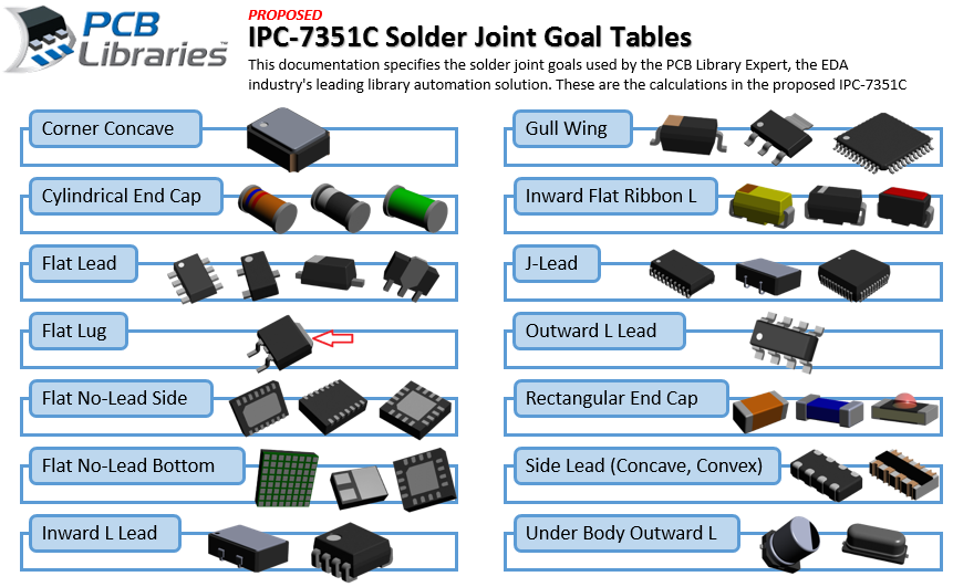 Here are the new Terminal Preferences in V2016.08:  |
|
 |
|

|
|
|
|
|
cioma
Advanced User 
Joined: 17 Jul 2012 Status: Offline Points: 150 |
Post Options
Thanks(0)
Quote Reply
Posted: 05 Jul 2016 at 12:54am |
|
Many thanks for your and your team's efforts, Tom! It seems PCB Libraries.dat preference file is not available in the latest v2016.08.05 pre-release. Is there a way we could try out new settings now? |
|
|
|
|
Tom H
Admin Group
Joined: 05 Jan 2012 Location: San Diego, CA Status: Offline Points: 6075 |
Post Options
Thanks(0)
Quote Reply
Posted: 13 Jul 2016 at 5:05am |
|
V2016.08 is released if you want to try it out - www.pcblibraries.com/downloads
|
|
|
|
|
martin.s
New User 
Joined: 17 Nov 2015 Status: Offline Points: 3 |
Post Options
Thanks(0)
Quote Reply
Posted: 13 Jul 2016 at 11:56pm |
|
Wasn't there the proposal to take the height of chip components into consideration? I can not find a hint to that in the Solder Joint Goal excel file.
|
|
|
|
|
Tom H
Admin Group
Joined: 05 Jan 2012 Location: San Diego, CA Status: Offline Points: 6075 |
Post Options
Thanks(0)
Quote Reply
Posted: 12 Sep 2016 at 9:22am |
|
The chip height was ruled out primarily because of multiple component sources required for each part number. If Height was used to create a land pattern for a 0805 capacitor, you could never find 3 sources with the same package Height. The 0805 Capacitor has at least a dozen different heights ranging 0.50 mm to 2.00 mm. This would create 12 different land patterns just for a 0805 Capacitor and designers and EE engineers want a single 0805 pattern so that multiple sources can be used. Using Height to determine a land pattern will be popular in the future because it nails down a perfect pattern for a specific package. But then, you have to provide the inventory for that package to assembly so that they do not substitute a different package. Using Height to determine a land pattern would dramatically increase the number of different patterns in everyone's CAD library and the industry is not ready for that yet. |
|
|
|
|
eFBe
New User
Joined: 07 Mar 2018 Status: Offline Points: 1 |
Post Options
Thanks(0)
Quote Reply
Posted: 07 Mar 2018 at 10:43am |
|
Hi Tom,
this may be too late reaction to your previous post, but it's still to the point I think. You argue that 0805 Capacitor has too much different heights and EE engineers want single 0805 land pattern. I don't know much about other engineers needs, but decision between lower quantity of land patterns and higher land pattern precision (and higher quantity of course) should be up to everyone of us. The fact that relation between component height and land pattern dimension is considerable leads me to create separate land pattern to every component with it's specific height. I absolutely don't care about quantity of land patterns. I just want to have accurate land patterns. Is it somehow possible to configure PCB Library Expert to take the height of the component into account during the calculation of land pattern? If it is not possible now, do you plan to integrate this functionality in the future? Besides this problem I like the free version of PCB Library Expert tool and considering purchase of Enterprise version, but this may be a deal breaker for me. |
|
|
|
|
Tom H
Admin Group
Joined: 05 Jan 2012 Location: San Diego, CA Status: Offline Points: 6075 |
Post Options
Thanks(0)
Quote Reply
Posted: 07 Mar 2018 at 10:56am |
|
Various heights in an 0805 Capacitor have no impact on the land pattern. One pattern can be sufficient for all 0805 Capacitors.
The IPC-J-STD-001 standard for solder joint acceptability states that the Maximum Toe value for every electronic package should not exceed 0.50 mm. If if does exceed 0.50 mm then the solder will simply melt on the pad rather than forming a fillet up the side of the terminal lead. The IPC-J-STD-001 indicates that the Toe solder joint should be a minimum of 25% of the terminal lead height. The big issue today with package height is 3D STEP models. While you can have a single land pattern for every 0805 Capacitor, you will need a 3D STEP model for every 0805 Height. The Land Pattern Name and the 3D STEP model name are normally the same to eliminate errors. V2018 Library Expert has different solder joint goals for 01005, 0201, 0402, 0603, 0805, 1206, etc. and these values are all user definable, but only in Library Expert Enterprise. |
|
|
|
|
mansour88
New User
Joined: 08 Aug 2019 Status: Offline Points: 1 |
Post Options
Thanks(0)
Quote Reply
Posted: 08 Aug 2019 at 4:19pm |
|
Hi,
Since we are talking about taking height into consideration, if you were to design a footprint for a part with really thick leads, like a L-shape wire terminal with AWG of 20, would you extend the pad length for a better solder fillet?
Is there any rule of thumb in this situations? I was looking at IPC-7351 and couldn't find any info that relates the lead thickness to the pad size.
|
|
|
|
|
Tom H
Admin Group
Joined: 05 Jan 2012 Location: San Diego, CA Status: Offline Points: 6075 |
Post Options
Thanks(0)
Quote Reply
Posted: 09 Aug 2019 at 9:25am |
|
The Terminal Lead Thickness (Not the Package Height) has an impact on the "Toe" value.
The Toe does not have to be any longer than the Terminal Lead Thickness and IPC-J-STD-001 (for assembly acceptance) indicates that the Toe solder should be a minimum 25% of the lead thickness or a maximum of 0.50 mm, whichever is greater. Therefore, regardless of the Terminal Lead Height, the maximum Toe value for Pad size calculation is 0.50 mm. Here is an example of a Gull Wing Terminal Lead and the calculation of the Toe value.  Note: the Toe can be longer, but it's unnecessary and consumes valuable PCB real-estate. Longer Toe values push out the placement courtyard. |
|
|
|
|
lsday
Active User 
Joined: 15 Dec 2014 Status: Offline Points: 24 |
Post Options
Thanks(0)
Quote Reply
Posted: 11 Sep 2019 at 2:17pm |
|
I like the new solder joint goals. What I don't like too much is that the pads don't calculate to even numbers.
|
|
|
|
|
Post Reply
|
Page 12> |
| Tweet |
| Forum Jump | Forum Permissions You cannot post new topics in this forum You cannot reply to topics in this forum You cannot delete your posts in this forum You cannot edit your posts in this forum You cannot create polls in this forum You cannot vote in polls in this forum |


 Topic Options