

|
|
Naming Convention for Odd shaped padstacks |
Post Reply 
|
| Author | |
budnoel 
Active User 

Joined: 16 Mar 2012 Status: Offline Points: 17 |
 Post Options Post Options
") Thanks(0) Thanks(0)
 Quote Reply Quote Reply
 Topic: Naming Convention for Odd shaped padstacks Topic: Naming Convention for Odd shaped padstacksPosted: 05 Nov 2012 at 11:44am |
|
Allegro PCB Editor has the ability to create Odd shaped padstacks and associate them with pins within the symbol. I was wondering about naming conventions however. What would you recommend for the padstack name associated with the Drain on this MOSFET? |
|
 |
|

|
|
|
|
|
Tom H
Admin Group 

Joined: 05 Jan 2012 Location: San Diego, CA Status: Offline Points: 6075 |
Post Options
Thanks(0)
Quote Reply
Posted: 05 Nov 2012 at 12:24pm |
|
The footprint name would be - SON_ALPHA&OMEGA_AON742 Component Family _ Mfr. Name _ Mfr. Part Number So your library will always sort on the component family and then the Mfr. and then the Part Number. |
|
|
|
|
budnoel
Active User
Joined: 16 Mar 2012 Status: Offline Points: 17 |
Post Options
Thanks(0)
Quote Reply
Posted: 05 Nov 2012 at 12:28pm |
|
Thanks Tom but I was wondering about the padstack name, not the symbol name. The padstack for the drain on this MOSFET is a very odd shape. The view in the data sheet makes appear to look like a castle with 4 turrets. |
|
|
|
|
Tom H
Admin Group
Joined: 05 Jan 2012 Location: San Diego, CA Status: Offline Points: 6075 |
Post Options
Thanks(0)
Quote Reply
Posted: 05 Nov 2012 at 12:41pm |
|
There is no IPC standard padstack name for a user defined contour (irregular) pad shape.
But I guess we're going to have to figure one out once we get to the export part of our new "Package Editor" which will allow you to easily create this library part in the V2013 PCB Footprint Expert. Maybe we'll have to leave the irregular padstack field open for the User to define. This is highly customized with many (17) vertexes. 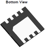 |
|
|
|
|
DaveCowl
Advanced User 

Joined: 18 Oct 2012 Location: Santa Clara, CA Status: Offline Points: 161 |
Post Options
Thanks(1)
Quote Reply
Posted: 05 Nov 2012 at 7:00pm |
|
I have FETs with similarly large numbers of vertices in some of my designs... looking forward to a consistent naming scheme also. BTW, I joined the 'family' for real today with my purchase - really looking forward to where this is all going...!
|
|
|
|
|
Nightwish
Active User

Joined: 20 Feb 2012 Location: Shanghai China Status: Offline Points: 33 |
Post Options
Thanks(0)
Quote Reply
Posted: 06 Nov 2012 at 12:33am |
|
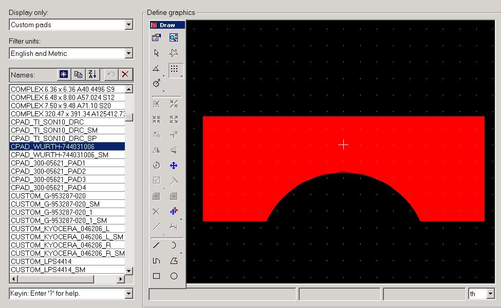
For odd shape or irregular shape pad our naming convention is CPAD_CELL NAME. The picture show an example to this. CPAD means it is custom defined pads. The padstack is used for a WURTH inductor. If we want the Solder mask or paste different than the pad we choose to add a suffix _SM or _SP to the padstack name.
 Thanks,
Nightwish
|
|
|
|
|
AGONZ67
Committee 

Joined: 30 Mar 2012 Status: Offline Points: 122 |
Post Options
Thanks(0)
Quote Reply
Posted: 06 Nov 2012 at 1:08pm |
|
I use a similar naming fashion, just the mfr&series for example JOHNSON_142-0711201-L where the L means left if required. The "CPAD" may be redundant because the pad is already in the "custom pads" partition.
|
|
|
|
|
Post Reply
|
|
| Tweet |
| Forum Jump | Forum Permissions You cannot post new topics in this forum You cannot reply to topics in this forum You cannot delete your posts in this forum You cannot edit your posts in this forum You cannot create polls in this forum You cannot vote in polls in this forum |


 Topic Options