|
|
J-STD-001: Plated Through-hole Obstruction |
Post Reply 
|
| Author | |
Tom H 
Admin Group 

Joined: 05 Jan 2012 Location: San Diego, CA Status: Offline Points: 6074 |
 Post Options Post Options
") Thanks(0) Thanks(0)
 Quote Reply Quote Reply
 Topic: J-STD-001: Plated Through-hole Obstruction Topic: J-STD-001: Plated Through-hole ObstructionPosted: 15 May 2017 at 6:25pm |
|
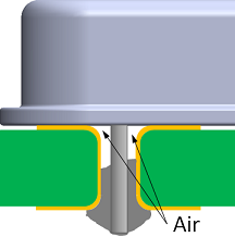
IPC-J-STD-001 identifies Hole Obstruction as “Parts and components shall be mounted such that they do not obstruct solder flow onto the solder destination side lands (pads) of plated through holes (PTH’s) required to be soldered”. Example of Hole Obstruction:
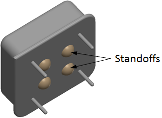
This issue pertains to through-hole terminals that are under the component package where the bottom of the package sits directly on the PCB surface and can be resolved by simply lifting the component package slightly off to PCB surface. IPC-J-STD-001 states minimal acceptable conditions for supported holes for through-hole terminals are Acceptable for Class 1, Process Indicator for Class 2 (means the assembly process can be improved) and a Defect for Class 3. The solder for PTH parts should reveal “Visible Wetting” on the top side of the PCB. To avoid Hole Obstruction, component manufacturers are forming the package body to lift it off the PCB allowing the Air in the hole to be pushed out and form an adequate solder joint. 4-pin PTH Oscillator with bottom side bumps:
LED with Lead Stops to prevent the component body from touching the PCB:
Radial
Capacitor with Kinked Leads to be able to inspect “Visible Wetting”:
|
|
 |
|

|
|
|
|
|
JamesUS
New User 
Joined: 26 Jun 2017 Status: Offline Points: 6 |
Post Options
Thanks(0)
Quote Reply
Posted: 12 Aug 2017 at 7:07am |
|
Hello, I am beginner to Soldering and IPC Training, as I know the IPC J-STD-001 is a training program which require learning the material in the J-STD-001 specification related to various assembly methods. When I needed some help related to soldering I usually go to www.ipctraining.com.
|
|
|
|
|
Anderson
Active User 
Joined: 10 Feb 2017 Status: Offline Points: 16 |
Post Options
Thanks(0)
Quote Reply
Posted: 06 Oct 2017 at 2:46am |
|
I learned many things till now online but I want to know more, specifically want to get practical knowledge. Is there any blog or tutorials you want to refer me?
|
|
|
|
|
Tom H
Admin Group
Joined: 05 Jan 2012 Location: San Diego, CA Status: Offline Points: 6074 |
Post Options
Thanks(0)
Quote Reply
Posted: 06 Oct 2017 at 6:55am |
|
There are some PCB Layout notes that I created here - https://blogs.mentor.com/tom-hausherr/
More will be coming. |
|
|
|
|
Post Reply
|
|
| Tweet |
| Forum Jump | Forum Permissions You cannot post new topics in this forum You cannot reply to topics in this forum You cannot delete your posts in this forum You cannot edit your posts in this forum You cannot create polls in this forum You cannot vote in polls in this forum |


 Topic Options