

|
|
IPC-7093A BTC: QFN Solder Mask Defined Thermal Pad |
Post Reply 
|
| Author | |
Tom H 
Admin Group 

Joined: 05 Jan 2012 Location: San Diego, CA Status: Offline Points: 5716 |
 Post Options Post Options
") Thanks(1) Thanks(1)
 Quote Reply Quote Reply
 Topic: IPC-7093A BTC: QFN Solder Mask Defined Thermal Pad Topic: IPC-7093A BTC: QFN Solder Mask Defined Thermal PadPosted: 30 May 2017 at 7:07am |
|
For the past decade, PCB designers created parts with thermal tabs with a 50% paste mask reduction checker board pattern. Then they inserted vias through the Thermal Pad and the holes sometimes intersected the Paste Mask. The thermal pad solder mask was 1:1 scale of the thermal pad. During reflow the paste would melt and travel down the via holes.
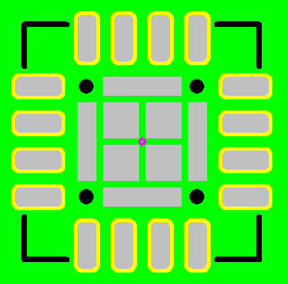
The PCB designer might have created a fabrication note to plug the holes on the Thermal Pad not knowing that it would increase cost by 10 - 15% just for a single BTC (Bottom Terminal Component. Plugged Via:  Here is an illustration of a QFN with vias going through the Thermal Pad allowing solder to flow through them. This creates a couple problems. 1. With Lead-free solder and having the PCB in the reflow oven twice as long as Lead solder, the entire PCB heats up and the solder may go all the way through the via hole and come out the bottom side causing solder protrusion. 2. When the solder goes into the vias, it robs the thermal pad from having the optimal solder joint. Less solder = bad connection. 3. The thinner PCB thickness of 1 mm can be problematic because it's easier for the solder to flow out the bottom side and could cause shorting. Old Thermal Pad Paste Mask with 50% reduction:  Note: all vias in a Thermal Pad must have a direct connection to the GND plane. Using Thermal Relief patterns with defeat the purpose of heat reduction away from the BTC component. 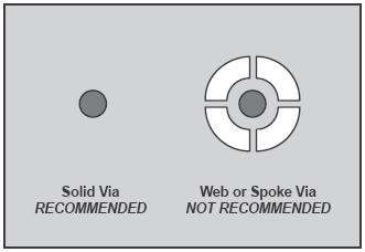 The new updates to upcoming revision to IPC-7093 will be teaching PCB designers to create a Solder Mask Defined Thermal Pad to create solder dams between the checker board pattern and around the vias to prevent solder from flowing down open via holes. No need to plug these vias and save fabrication costs at the same time creating a reliable solder joint. Here is the Land Pattern in the CAD tool illustrating the Solder Mask layer on top. In the CAD tool, Solder Mask areas in Yellow are “absence of solder mask” as that CAD layer in a Negative image. The Green areas are solder mask. 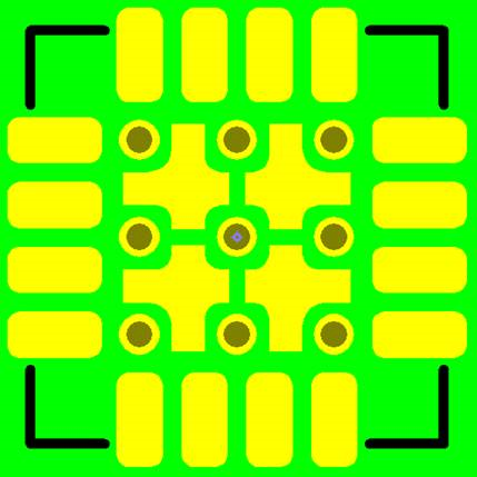 Here is the Land Pattern in the CAD tool illustrating the Paste Mask layer on top. This layer is a Positive image. The Gray areas are Paste Mask. The Yellow area is the solder mask swell. The Green area is the solder mask. The Black lines are Legend outlines. The Black dots are the via holes. 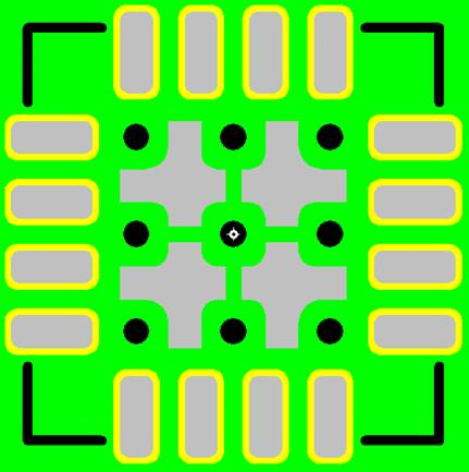 Dimensional Details: 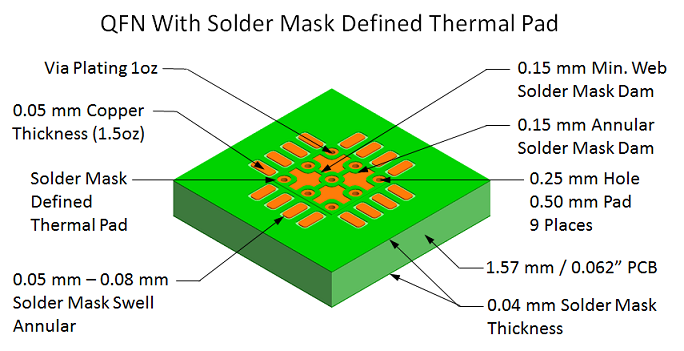 QFN Pattern with 0.10 mm (4 mil) Paste Mask: 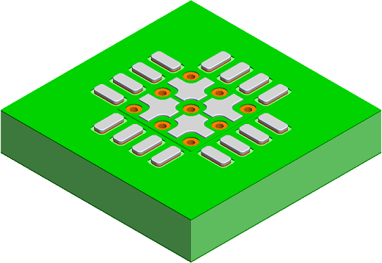 Space the vias evenly. Random via location makes the solder mask defined thermal pad much more complex to create symmetrical paste mask aperture openings. For the balancing of the package during reflow, it's important to have even paste mask distribution. The minimum via pitch is 0.80 mm. 9 vias is good enough to draw the maximum amount of heat away from the BTC. If you insert more than 9 vias, the heat reduction is insignificant. However, if you insert less, the heat dissipation transfer declines and less vias could increase the electrical impedance to GND which in turn affects the device power and signal integrity. Here is a CAD tool sample of a thermal pad with 4 vias: Green = Solder Mask Yellow = Solder Mask Opening Gray = Paste Mask Black Dots = 0.30 mm via holes to GND plane for 4 vias
 Here is a CAD tool sample of a thermal pad with 5 vias: Vias hole size = 0.25 mm for 5 vias 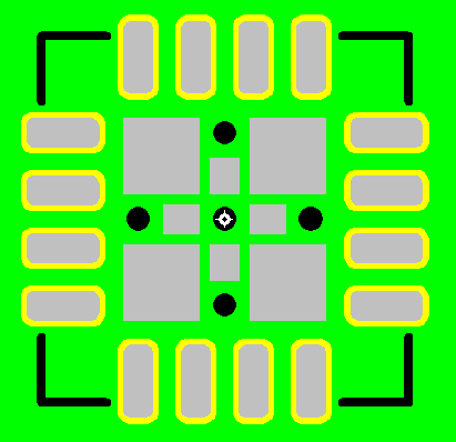 Here is a CAD tool sample of a thermal pad with 9 vias: Vias hole size = 0.20 mm for 9 vias 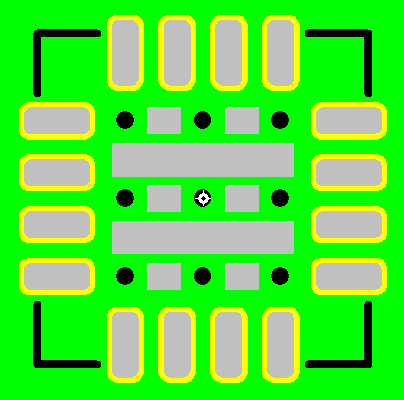 There is some really good information about this subject authored by Matt Kelly, Mark Jeanson and Mitch Ferrill from IBM. Read this in-depth presentation on BTC technology. IBM BTC VIP Article Here |
|
 |
|
|
|
|
Tom H
Admin Group
Joined: 05 Jan 2012 Location: San Diego, CA Status: Offline Points: 5716 |
Post Options
Thanks(0)
Quote Reply
Posted: 02 Jan 2020 at 11:53am |
|
Here are the rules for the SON with a Thermal Pad that touches the signal pads.
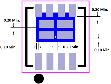 Note: these are minimum values. There are no maximum values, but you should maintain at least 50% paste make coverage on the thermal pad. |
|
|
|
|
SWB01
Active User 
Joined: 24 Mar 2013 Status: Offline Points: 41 |
Post Options
Thanks(0)
Quote Reply
Posted: 02 Jan 2020 at 11:13pm |
|
|
|
Tom H
Admin Group
Joined: 05 Jan 2012 Location: San Diego, CA Status: Offline Points: 5716 |
Post Options
Thanks(0)
Quote Reply
Posted: 03 Jan 2020 at 8:55am |
|
Yes, the On Semiconductor AND9137/D recommended footprint has a 0.25 mm spacing between paste mask apertures.
I see some designers overlap the thermal tab paste mask with the signal pin paste mask and that stencil will not work. The stencil webbing needs to be robust if you want the stencil to last longer and work correctly.
|
|
|
|
|
Tom H
Admin Group
Joined: 05 Jan 2012 Location: San Diego, CA Status: Offline Points: 5716 |
Post Options
Thanks(1)
Quote Reply
Posted: 16 Feb 2021 at 9:42am |
|
|
|
Post Reply
|
|
| Tweet |
| Forum Jump | Forum Permissions You cannot post new topics in this forum You cannot reply to topics in this forum You cannot delete your posts in this forum You cannot edit your posts in this forum You cannot create polls in this forum You cannot vote in polls in this forum |


 Topic Options