 LEAP
LEAP - Libraries Enhanced by Automated Preferences
The
Footprint Expert is based on
CAD LEAP technology. This allows synchronization of component package dimensions with user definable Options, enabling the standardization and enforcement of library rules throughout your organization. There are dozens of configurable Options that can be modified to your organization's specific requirements, which may in turn be shared across your company, division, and even outsource partners. This will enable you to have a consistent, high-quality library of footprints with reliable solder patterns standardized across all design and production. If you have not seen the
Footprint Expert, you have never seen anything like this before.
The PCB Footprint Expert makes your footprint part library adjustable so it can be standardized by these Option features:
1. Units- Millimeters, Micrometers, Inches and Mils
- Component Package dimension unit accuracy
- Minimum for the absolute minimum value is normally 2 places to the right of the decimal. Standard package dimensions have minimum units in 0.01 increments.
- Maximum for the maximum value defaults to 3 places or 0.001 increments. Users who want higher resolution can change the maximum value to 4 places or 5 or 6 places. Higher resolution makes switching from metric to imperial measurements more accurate.
- Calculated Footprint dimension unit accuracy
- Minimum for the absolute minimum value for pad stack dimensions is normally 2 places to the right of the decimal. Pad stack dimensions have minimum units in 0.01 increments. A resolution of 1 would produce pad stack dimensions in 0.10 increments. The values would be rounded up/down to the nearest 0.10. numbers 1 - 4 would round down and 5 - 9 would round up. Example: 0.53 would round down to 0.50 and 0.56 would round up to 0.60. The resulting pad stack would be a maximum of +/- 0.04 different than a 2-place pad stack.
- Minimum for the absolute minimum value for pad place dimensions is normally 3 places to the right of the decimal or 0.001 increments. A pad place resolution of 2 would place the pad centers on a 0.01 grid and a pad place resolution of 1 would place the pad centers on a 0.10 grid
2. The footprint name is auto generated using these options:
- PCB Libraries (approved for the unreleased IPC-7351C)
- IPC-7351B
- IPC-7352
- Custom (personal)
3. Density Levels - include or exclude density level suffix in footprint name
- Least (L)
- Nominal (N)
- Most (M)
4. Solder Mask settings:
- Minimum solder mask web value
- Gang Mask when rule is violated
- Solder mask expansion value
- 1:1 scale would allow fabrication to expand to meet their application tolerance
- Separate controls for thermal tab solder mask expansion
- Separate controls for through-hole solder mask expansion
5. Paste Mask settings:
- Annular +/- Expansion by percentage
- Annular +/- Expansion by value
- Thermal pads paste mask percent reduction
- Thermal pad paste mask percent ranges from 40 - 70%
- Minimum thermal pad paste mask pattern spacing
- Pin-in-Paste technology for through-hole pad stacks
6. Pad Shapes:
- Oblong - recommended in IPC-7351B
- Rectangle - recommended by component manufacturers
- Rounded Rectangle - recommended for PCB assembly shop stencil apertures
- D-Shape - many PCB CAD tools do not natively support this pad shape
- Round - BGA, CGA, LGA and every through-hole component
- Square - LGA and Pin 1 for through-hole components
7. Pad Trim and Spacing Rules:
- Minimum pad to pad spacing
- Minimum pad to thermal pad spacing
- Minimum trim stand-off height for gullwing terminals
8. Drafting Outlines:
- Silkscreen
- Line width for different density levels (plus on/off switch)
- Map outline to minimum, nominal and maximum package dimensions
- Pad clearance gap
- Ref des height and width (plus on/off switch)
- Pin 1 polarity marking min/max diameter
- Assembly
- Line Width (plus on/off switch)
- Map outline to minimum, nominal and maximum package dimensions
- Pin 1 polarity marker
- Minimum and Maximum Ref des height and width (plus on/off switch)
- Add outlines to pad stack (filled or outline)
- Courtyard
- Line Width (plus on/off switch)
- Expand to include silkscreen
- Different settings for package body and pad stacks
- Contoured or rectangle outline
- Minimum cut-in gap
- Origin
- Line Width
- Crosshair size (plus on/off switch)
- Target diameter (plus on/off switch)
- Component and Terminals
- Component Line Width (plus on/off switch)
- Terminal Line Width (plus on/off switch)
9. Layer Options
- Turn layers on/off
- Change layer color assignments
- Assign layer visibility hierarchy
10. 3D Colors
- Define color assignments for every component family
- Primary body
- Secondary body
- Default terminal leads
- Pin 1 terminal lead
- Polarity dot
11. Component Families
- Set rotation for Pin 1 location
- Lower Left
- Lower Right
- Upper Right
- Upper Left
- Set Origin Location
12. Terminal Settings:
- Surface Mount
- Toe, Heel and Side solder joint goals
- Least, Nominal and Most density levels
- Courtyard Excess
- Through-hole
- Courtyard Excess
- Hole Excess over round lead
- Hole Excess over rectangular lead
- Hole size round-off
- Minimum annular ring
- Pad-to-Hole ratio
- Pad-to-Slot ratio
- Pad size round-off
- Plane anti-pad excess over hole
- Plane thermal relief ID/OD
- Thermal relief spoke width
- Wave solder keep out
Define all these Option preferences to create your personal CAD library with construction consistency, regardless of how many people are involved in CAD library creation process. Having a PCB CAD library that uses the same preference rules greatly enhances the PCB design appearance and accuracy.
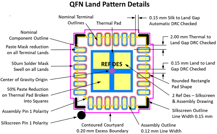
Example of all the preference option elements that come together with the component package dimensions to auto-generate the perfect solder pattern and 3D STEP model for your CAD library.
Besides a perfect footprint, the Component Package Dimensions also enable the Footprint Expert to produce a matching, detailed 3D STEP model:
PCB Footprint Expert
To get a fully functional Footprint Expert license, complete the Evaluation License request on the Downloads page. Make sure to provide all the requested information, such as your company details and CAD outputs needed.
Get your FREE Footprint Calculator or Footprint Expert Evaluation License:
Call: 847-557-2300


 Post Options
") Thanks(0)
Thanks(0)
 Quote
Quote  Topic: CAD LEAP Technology


 Topic Options