In the
Manufacturer Recommended Patterns technical paper (
link here), we discussed the importance of drafting outlines because the component manufacturers that provide recommended solder patterns do not provide information regarding this subject. This includes Standard and Non-Standard component packages.
These Drafting Outlines are Auto Generated in Footprint Expert and 100% user controlled:
- Silkscreen Outline, Reference Designator and Pin 1 Polarity Dot
- Assembly Outline, Reference Designator and Polarity Chamfer
- Courtyard Excess (Contoured or Rectangle)
- Origin Marker (Crosshair and Target)
- Component and Terminals
- Assembly Pads
1. Silkscreen Outlines and Reference Designators for 3 Density Levels Most, Nominal and Least
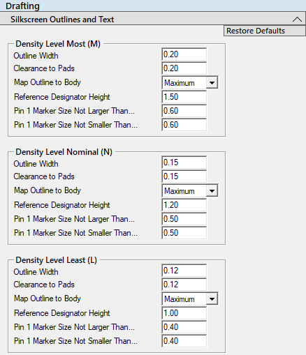
Silkscreen outlines and reference designators are included in the PCB fabrication output files. The following rules can be applied separately to each Density Level. It is important to note that in most fabrication shops the minimum legend line width is 0.10.

a. Outline Width Default Settings (user definable)
- Most Density default width is set to 0.20
- Nominal Density default width is set to 0.15
- Least Density default width is set to 0.12
Note: if you make the silkscreen legend too thick, it will push the Courtyard out and consume more PCB space and limit the part placement. We recommend 0.20 for the thickest legend line width and 0.10 for the thinnest and 0.15 for the average.
b. Clearance to Pads
- This rule must consider the solder mask expansion annular ring and add 0.10 to that value. If your solder mask annular ring is 0.05 + 0.10 = 0.15 pad to silkscreen gap. Appling the silkscreen to the PCB has a 0.05 misalignment tolerance and the minimum silkscreen to solder mask rule is 0.05.
c. Map Outline Body
- Maximum (default setting)
- Nominal
- Minimum
d. Reference Designator Height
- Most Density default height is set to 1.50
- Nominal Density default height is set to 1.20
- Least Density default height is set to 1.00
e. Pin 1 Marker Size Not Larger Than... (defaults)
- 0.60 - Density Level Most (M)
- 0.50 - Density Level Nominal (N)
- 0.40 - Density Level Least (L)
f. Pin 1 Marker Size Not Smaller Than... (defaults)
- 0.60 - Density Level Most (M)
- 0.50 - Density Level Nominal (N)
- 0.40 - Density Level Least (L)
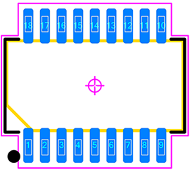
The CAD librarian can enter different values for the "Not Larger Than" and "Not Smaller Than" the program will auto-size the dot per the pad width. The smallest polarity dot visible on the PCB without magnification is 0.40. The silkscreen polarity dot is placed to the left of Pin 1 because the end of pin 1 could be a via location. Avoid placing silkscreen in potential via locations.
Here is an example of a 0.65 mm pitch SOP with a 0.50 Pin 1 Dot.
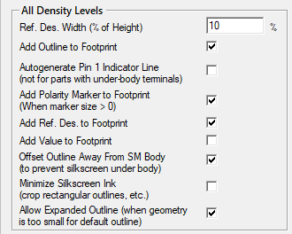
2. Silkscreen Settings All Density Levels
a. Ref. Des. Width (% of Height)
- This feature is used for "Stroke" font.
- The default setting is 10% of the ref des height. Larger percentages can cause character bleeding, making the letters illegible on the PCB.
b. Add Outline to Footprint (on-off)
- The default is On, but some companies do not put silkscreen legend on final PCBs
- You can build an entire PCB library with legend and one without
c. Autogenerate Pin 1 Indicator Line
- This feature draws a legend line next to Pin 1. Many designers use this instead of the pin 1 dot as it is located inside the placement courtyard. Note: this feature is only applicable for external terminal leads and not used for BTC (Bottom Termination Components) like Grid Arrays or QFN, SON, DFN packages.
- Here is an example of a 0.65 mm pitch SOP with a Pin 1 Indicator Line:
d. Add Polarity Marker to Footprint (on/off)
- (When marker size > 0)
- The default is On
e. Add Ref. Des. to Footprint (on/off)
f. Add Value to Footprint (on/off)
g. Offset Outline Away from SM Body
- The default is On. Places silkscreen outline outside the component body.
h. Minimize Silkscreen Ink (crop rectangle Outlines)
- Unchecked equals a Full Silkscreen outline
- Checked equals a Hatched Silkscreen outline
i. Allow Alternate Outline (when geometry is too small for default outline)
- Unchecked equals no silkscreen outline if the footprint is too small
- Checked equals a wraparound silkscreen outline if the footprint is too small
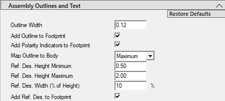
3. Assembly Outlines and Text
- Default value is set to 0.12, but users change this value for their own custom library
b. Add Outline to Footprint (on/off)
- The default setting is On
c. Add Polarity Indicators to Footprint (on/off)
- This feature adds a polarity chamfer in the outline to the corner where Pin 1 is located. The default setting is On
- Maximum (default setting)
This means that the legend outline will map to the maximum package dimensions - Nominal
- Minimum
e. Ref. Des. Height Minimum
- Footprint Expert auto-sizes the ref. des. height to fit in the middle of the assembly outline. The default minimum value is 0.50.
f. Ref. Des. Height Maximum
- The default maximum value is 2.00
g. Ref. Des. Width (% of Height)
- This feature is only used for the CAD tool "Stroke" font. It is not used for Windows text fonts. The default value is 10%.
h. Add Ref. Des. to Footprint (on/off)
- The default setting is On
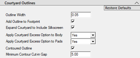
- The default value is 0.05
b. Add Outline to Footprint (on/off)
- This feature turns the courtyard outline on or off. The default setting in On.
c. Expand Courtyard to Include Legend (on/off)
- The default setting is On
d. Apply Courtyard Excess Option to Body (Yes/No)
- This feature applies the Courtyard Excess to Body or turns it off.
e. Expand Courtyard Excess Option to Pads (Yes/No/Ignore)
- This feature applies the Courtyard Excess to Pads or turns it off or Ignores pads.
f. Contoured Courtyard (on/off)
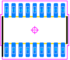
- This feature selection is contoured outlines (on) or rectangular outlines (off):
- Contoured On
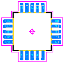
- Contoured Off
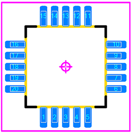
g. Minimum Courtyard Cut-in Gap
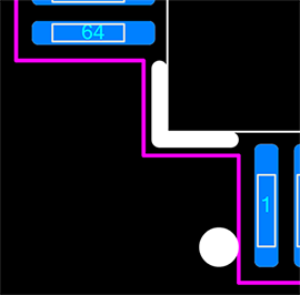
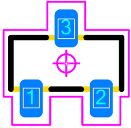
- The default value is 5.00. This feature allows the courtyard outline to cut in-between pads of whatever value you set. If the cut-in gap is 1.00 then the courtyard will contour between pads that have greater than 1.00 separation. Cut-in Gap 5.00
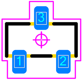
Cut-in Gap 0.50. The courtyard cut-in between pins 1 & 2
5. Origin Outlines- The default line width setting is 0.05
- The default value is 0.70
c. Add Crosshair to Footprint (on/off)
- The default setting in On
- The default value is 0.50
e. Add Origin Target to Footprint (on/off)
- The default setting in On
6. Component and Terminal Outlines
a. Component Outline Width
- The default value is 0.025
b. Include Comp. Outline in CAD Output (on/off)
- The default setting is On
c. Terminal Outline Width
- The default value is 0.025
d. Include Terminals in CAD Output (on/off)
- The default setting is On
Terminal Outlines
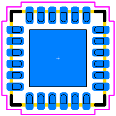
PCB Footprint Expert
The Footprint Expert will generate your footprints with accurate, consistent, reliable drafting outlines to minimize chances of human error. Modify a setting, then batch-rebuild your entire library! The Footprint Expert helps you create flawless PCB designs much more efficiently!
Get your FREE Footprint Calculator or Footprint Expert Evaluation License:
Call: 847-557-2300


 Post Options
 Thanks(0)
 Quote
Quote  Reply
Reply
 Topic: Drafting Outline Options