

 |

|
Ball Grid Array |
Post Reply 
|
| Author | |
Nick B 
Admin Group 
Joined: 02 Jan 2012 Status: Offline Points: 1931 |
 Post Options Post Options
 Thanks(0) Thanks(0)
 Quote Quote  Reply Reply
 Topic: Ball Grid Array Topic: Ball Grid ArrayPosted: 10 Jan 2025 at 11:25pm |
|
A Ball Grid Array (BGA) is a surface-mount package used for integrated circuits for CPU processors (FPGAs – Field Programable Grid Array) and memory chips (PBGA – Plastic Ball Grid Array). In this package, the terminal leads between the BGA package and the circuit board are made using small solder balls arranged in a grid pattern on the underside of the component. BGA solder balls are made of lead-free or lead-based solder, but the electronics industry is trying to eliminate lead-based solder. A key feature of BGA packaging is a smaller footprint, with usually a smaller space to pin quantity ratio. BGA packages are more compact and allow for higher pin counts in smaller areas compared to other package types like Quad Flat Package (QFP). 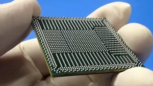 BGA packages are commonly used in electronic devices like cell phones, computer mother boards, and other high-performance consumer electronics. The construction of a Ball Grid Array (BGA) involves several layers and components that make up the overall package, which is used to connect an integrated circuit (IC) to a printed circuit board (PCB).
There is also a Solder Mask Defined BGA that has solder mask over the pad edges. The annular ring of the solder mask on pad is typically 0.05 mm. This technology is primarily used to secure the PCB pad to the PCB prepreg in handheld devices like cell phones. During drop tests, the solder joint between the BGA ball and the pad remains intact, but the pad could separate from the prepreg. Solder mask and prepreg are both epoxy resin (glue). The solder mask will help secure the pad to the prepreg to prevent the pad separating from the prepreg. This solder mask defined concept is primarily used on BGA pin pitches of 0.65 mm and lower, where the non-collapsing pad size is larger than the BGA ball diameter. 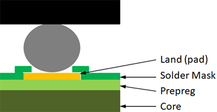 The primary reason for making the BGA pad size larger than the ball diameter is to accommodate via-in-pad technology because fine pitch BGAs cannot use the typical Dog-bone via fanout solution. 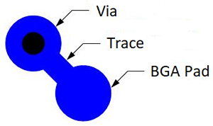 Via-in-Pad technology is a technique used in PCB design where the via is placed directly in the pad. This approach is commonly used in high-density interconnect (HDI) designs, especially for fine pitch BGAs. 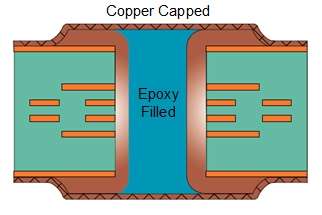 The via-in-pad (VIP) requires a separate fabrication process that includes plating, plugging and capping the hole and planarizing the capped pad to create a flat surface with no dimples. Capped pads with dimples create trapped air under the paste mask. When the PCB goes through the reflow oven, the trapped air in the pad dimple gets super-heated and blows through the solder and into the BGA ball causing a void. 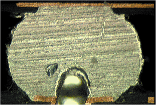 Most of the time the via-in-pad is a microvia that goes from the top layer to the first signal layer. Then buried vias connect to all the other inner layers. All BGA GND connections use microvias to Layer 2. However, PCB fabrication can now drill a hole with a 10:1 aspect ratio. A 1.57 mm thick PCB can support a via hole size of 0.15 mm. But the pad size must be 0.35 to support a 0.10 mm annular ring. This solution is good for 0.50 - 0.65 mm pitch BGAs. IPC-7351 provides BGA ball size tables with the reduction percentage for collapsing BGAs and the Increase for non-collapsing BGAs. IPC has a rule for BGA pad size tolerances. They take a Nominal Ball and reduce or increase the pad size by a percentage, then add a pad size tolerance (variation). IPC-7351 recommends using the Maximum Material Condition of the Variation (highlighted in Red). 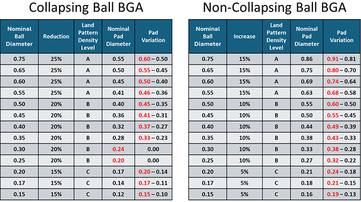 Footprint Expert uses these tables for BGA footprint calculations. However, every value is fully editable by the end user. Also, you can insert additional BGA ball diameters. Here are all the options that the Footprint Expert user can edit: 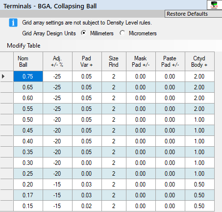 Over the years, BGAs have become increasingly complex, with large numbers of pins and all sorts of patterns. The Footprint Expert can help automate complex BGA footprints and 3D STEP models by allowing you to import CSV files (typically provided by component manufacturers), or keying in package dimensions. 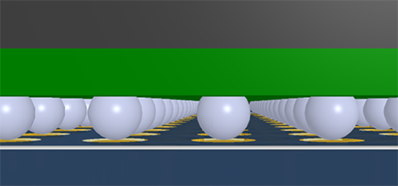 BGA Ball Materials The BGA ball may consist of a variety of metal alloys. Some of these include balls with some lead content such as 37Pb63Sn, 90Pb10Sn, 95Pb5Sn, while others do not contain lead such as Sn96.5Ag3.0Cu0.5, Sn96.5Ag3.5, Sn-9Zn-0.003Al. It is a good recommendation to use the same alloy, in a paste form, to attach the BGA balls to the mounting substrate; however, some of the balls that do not collapse require a paste that is more conducive to reflow temperatures. Lead-free balls have a combination of tin, silver and copper. This is the replacement for the tin/lead ball. BGAs are usually assembled using the standard reflow solder processes.  PCB Footprint Expert Simplify your PCB design process with the Footprint Expert, the ultimate tool for automating footprints and 3D STEP models for BGAs. Automation helps ensures accurate, consistent, reliable footprints with minimal introduction of human error. Let the Footprint Expert handle your CAD library so you can focus on creating flawless PCB designs faster and more efficiently! Get your FREE Footprint Calculator or Footprint Expert Evaluation License: Call: 847-557-2300 |
|
 |
|
 |
|
Post Reply 
|
|
| Tweet |
| Forum Jump | Forum Permissions  You cannot post new topics in this forum You cannot reply to topics in this forum You cannot delete your posts in this forum You cannot edit your posts in this forum You cannot create polls in this forum You cannot vote in polls in this forum |