
 |

|
SOTFL Side Calculation |
Post Reply 
|
| Author | |
caclark 
Advanced User 
Joined: 24 Oct 2012 Location: Cincinnati, OH Status: Offline Points: 177 |
 Post Options Post Options
 Thanks(0) Thanks(0)
 Quote Quote  Reply Reply
 Topic: SOTFL Side Calculation Topic: SOTFL Side CalculationPosted: 04 Oct 2013 at 5:23am |
|
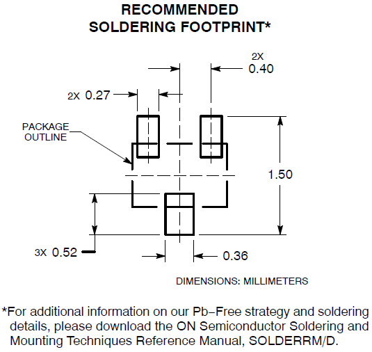
I am currently trying to calculate a SOTFL package (ON-Semi DTC114EM3). I was trying to adjust the "Side" fillet calculation for our very high shock application needs (beyond IPC Most) but the pad size does not change no matter the values put into this field.
The "Toe" and "Heel" pad sizes do change as expected when I input the values required. I am using PCB Library version: 2013.14 I think in general this part type in the calculator has some issues |
|
 |
|
 |
|
Jeff.M 
Admin Group 
Joined: 16 May 2012 Location: San Diego Status: Offline Points: 477 |
 Post Options Post Options
 Thanks(0) Thanks(0)
 Quote Quote  Reply Reply
 Posted: 04 Oct 2013 at 7:12am Posted: 04 Oct 2013 at 7:12am |
|
Check that the side isn't being trimmed to comply with your pad-to-pad clearance rule.
If that's not the problem please supply the values you're using so I can try to reproduce this condition.
|
|
 |
|
Tom H 
Admin Group 

Joined: 05 Jan 2012 Location: San Diego, CA Status: Offline Points: 5717 |
 Post Options Post Options
 Thanks(0) Thanks(0)
 Quote Quote  Reply Reply
 Posted: 04 Oct 2013 at 7:17am Posted: 04 Oct 2013 at 7:17am |
|
Can you attach a URL link to the package dimension datasheet?
I would like to take a look at this. Like Jeff mentioned, if your pad to pad spacing rule is set to a specific value the LE software will not override it until you select the "Footprint" tab and enter your own pad stack dimensions. |
|
 |
|
caclark 
Advanced User 
Joined: 24 Oct 2012 Location: Cincinnati, OH Status: Offline Points: 177 |
 Post Options Post Options
 Thanks(0) Thanks(0)
 Quote Quote  Reply Reply
 Posted: 07 Oct 2013 at 6:06am Posted: 07 Oct 2013 at 6:06am |
|
Here is the link to the datasheet:
http://www.onsemi.com/pub/Collateral/DTC114E-D.PDF And the particular package is on sheet 11 (SOT-723). Not only is it a SOTFL, but pin 3 is not the same width as pins 1 & 2. ( I am seeing this more and more lately on SOT parts, not exactly sure why but my guess would be so that the suppliers are trying to compensate pin 3 to have more surface area so that the part will stay centered better on the pads and not try to pull pin 3 off the pad during the reflow soldering process. (i.e. surface tension pull of pads 1 & 2 are approx same as pin 3) And as for the rules I was already assuming that it would not let me violate my user rule "Minimum Space Pad-to-Pad", so I even tool this value down to 0.05mm temporarily but no affect on the calculators outcome. It still will not change the pad width. As for the value I am trying to change the "Side" fillet is per J-STD-001 where all the fillets for "Flat Leads (FL)" pins have to be 100% the pin thickness. So in this case the nominal value for dim "c" on the datasheet is 0.12mm. (I usually try to use the max value (all our products are extremely "high shock" so we always try to error on the side of worst case condition), but in the case of this tiny part this would defiantly cause a Pin-to-Pin violation) |
|
 |
|
Tom H 
Admin Group 

Joined: 05 Jan 2012 Location: San Diego, CA Status: Offline Points: 5717 |
 Post Options Post Options
 Thanks(0) Thanks(0)
 Quote Quote  Reply Reply
 Posted: 07 Oct 2013 at 6:23am Posted: 07 Oct 2013 at 6:23am |
|
The issue here is that there is no IPC-7351 standard component family for SOTFL with different size component leads. So you can't use the SOTFL component family calculator to enter all the correct dimensions because it doesn't exist.
That is why PCB Libraries, Inc. created Footprint Designer (FP Designer) for these non-standard unique component packages that come with mfr. recommended solder patterns. And if you did not want to use the mfr. recommended pattern you could create your own pad stack sizes. This SOT-723 part should be built once in FP Designer and contributed to PCB Libraries so that no one has to build it again. Eliminate duplication of effort. Then you could take the existing footprint and modify the pad stack and auto-generate a new "custom" footprint in seconds.  |
|
 |
|
Post Reply 
|
|
| Tweet |
| Forum Jump | Forum Permissions  You cannot post new topics in this forum You cannot reply to topics in this forum You cannot delete your posts in this forum You cannot edit your posts in this forum You cannot create polls in this forum You cannot vote in polls in this forum |