

|
|
Add Ability for Arbitrary Irregular Shaped Pads |
Post Reply 
|
| Author | |
DaveCowl 
Advanced User 

Joined: 18 Oct 2012 Location: Santa Clara, CA Status: Offline Points: 161 |
 Post Options Post Options
") Thanks(0) Thanks(0)
 Quote Reply Quote Reply
 Topic: Add Ability for Arbitrary Irregular Shaped Pads Topic: Add Ability for Arbitrary Irregular Shaped PadsPosted: 12 May 2015 at 4:11pm |
|
I have a component that shows 4 regular rectangular pads but there is a non-plated through hole that sits between two of the pads and ideally I would like to cut a keepout into the pads (even though the manufacturer land pattern has the hole just cutting into the pads). The designer has a number of shape options but does not appear to allow for me to make a cut out other than a chamfer or similar. Any thoughts on whether this is possible in FPX, or do I need to make the modifications to the pad inside Allegro? Thanks! Dave.
|
|
 |
|
|
|
|
Tom H
Admin Group 

Joined: 05 Jan 2012 Location: San Diego, CA Status: Offline Points: 5716 |
Post Options
Thanks(0)
Quote Reply
Posted: 12 May 2015 at 4:14pm |
|
Send over a datasheet or a drawing that depicts what you want and I'll tell you away to accomplish that.
A drawing is worth a thousand words. |
|
|
|
|
DaveCowl
Advanced User
Joined: 18 Oct 2012 Location: Santa Clara, CA Status: Offline Points: 161 |
Post Options
Thanks(0)
Quote Reply
Posted: 12 May 2015 at 5:27pm |
|
This is the definition of the land pattern:
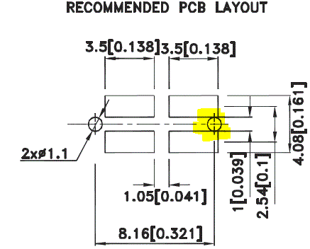 And this is the kind of land pattern I have seen for it: 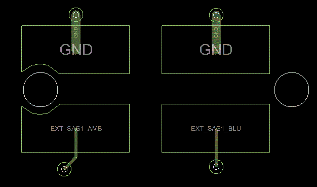 |
|
|
|
|
Tom H
Admin Group
Joined: 05 Jan 2012 Location: San Diego, CA Status: Offline Points: 5716 |
Post Options
Thanks(1)
Quote Reply
Posted: 12 May 2015 at 6:29pm |
|
Well, that is an exciting feature. I'll make a note of this when we design V2016 starting this July.
V2016 will be a complete re-write so we can add lots of new features, user preferences and rules. |
|
|
|
|
DaveCowl
Advanced User
Joined: 18 Oct 2012 Location: Santa Clara, CA Status: Offline Points: 161 |
Post Options
Thanks(0)
Quote Reply
Posted: 12 May 2015 at 6:31pm |
|
Yeah I thought it was an odd one... but no doubt something that comes up once in a while...
Cheers!
|
|
|
|
|
Maarten Verhage
Active User 

Joined: 27 Jul 2012 Location: Netherlands Status: Offline Points: 27 |
Post Options
Thanks(0)
Quote Reply
Posted: 13 May 2015 at 2:05am |
|
Hi Tom,
Are you willing to share a bit on the re-write of the software? Is it just the PCB Library Expert code or are you changing GUI libraries as well? Or other libraries your product depends on. The code is written in C++ right? Anyway, good luck to the software engineers. I hope the new architecture will turn out right so the new features would be easily implementable. Best regards, Maarten Verhage |
|
|
|
|
ernestorey
New User 
Joined: 10 Apr 2014 Location: Santa Clara, CA Status: Offline Points: 10 |
Post Options
Thanks(0)
Quote Reply
Posted: 13 May 2015 at 10:43am |
|
Dave, I'm curious about the part in question. What is the reason for an unplated hole in between the pads? Tooling holes so that the part does not get reversed? Seems too small for that and could create problems during P&P.
|
|
|
|
|
Tom H
Admin Group
Joined: 05 Jan 2012 Location: San Diego, CA Status: Offline Points: 5716 |
Post Options
Thanks(0)
Quote Reply
Posted: 13 May 2015 at 4:25pm |
|
Maarten... We're doubling our programming staff and upgrading to Windows 10 and Visual Basic 2015.
The new V2016 Library Expert will be a total rewrite and have double the features, such as schematic symbol editor and interactive graphic editing and measure features. Cutting a SMD pad around a non-plated hole will be easy. The trick is to make the next generation of PCB library automation powerful but easy to use. The GUI will be totally overhauled and no one will recognize it immediately, but it will have similar functionality. However, the new Library Expert will be light years ahead of any library editing tool in the electronics industry. One of the goals is to access POD directly from Library Expert to both upload and download FPX data. After V2015.12 there will not be any new features added but there will be bug fix releases for the rest of the year. We need to focus all programming effort on V2016 to meet the January 2016 release schedule. The current FPX format will translate into V2016 but then it will be reformatted for optimization. |
|
|
|
|
Post Reply
|
|
| Tweet |
| Forum Jump | Forum Permissions You cannot post new topics in this forum You cannot reply to topics in this forum You cannot delete your posts in this forum You cannot edit your posts in this forum You cannot create polls in this forum You cannot vote in polls in this forum |


 Topic Options