

|
|
Trimming heels under the component body |
Post Reply 
|
| Author | |
gcary 
Advanced User 
Joined: 06 Mar 2012 Location: USA Status: Offline Points: 69 |
 Post Options Post Options
") Thanks(0) Thanks(0)
 Quote Reply Quote Reply
 Topic: Trimming heels under the component body Topic: Trimming heels under the component bodyPosted: 06 Mar 2012 at 9:42pm |
|
Hi Tom and the rest of the forum members,
I recently posted to the Altium Designer forum regarding a land pattern in the Altium vault that has land pads that extend under the component body. In response, someone posted a link to a slide presentation that Tom Hausherr wrote that says that heel trimming is now deemed unnecessary. Here is a link to the document I'm referring to (page 19): http://communities.mentor.com/mgcx/servlet/JiveServlet/download/28883-8838/PCB%20Design%20Optimization%20Starts%20in%20the%20CAD%20Library.pdf Thanks for preparing this document. It has a lot of great information in it. Would you please explain the reason(s) why it isn't necessary to trim the heels? In the component I've been looking at, the A1 distance has a minimum value of 0.05mm, which would put the body of the component into the solder paste (assuming the component leads are pushed 0.05mm or more into the paste, which I expect it would). Thanks and regards, Greg |
|
 |
|
|
|
|
Tom H
Admin Group 

Joined: 05 Jan 2012 Location: San Diego, CA Status: Offline Points: 5716 |
Post Options
Thanks(1)
Quote Reply
Posted: 08 Mar 2012 at 12:07pm |
|
Greg,
Excellent question! The entire pad trimming under low profile Gull Wing components started when I took a J-STD-001 training class and the teacher pointed out this table 7-7 and Note 4 regarding the Heel Fillet - 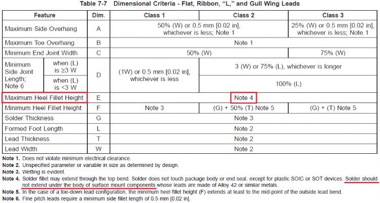 So we created the "K" dimension for the IPC-7351 standard to sync with J-STD-001. The problem was that we didn't read the entire line that states not to extend pads for "Component Leads Made of Alloy 42". So we added a new feature to the LP Calculator thinking that we were saving the world from under body solder joint short circuits, but the fact is no one ever reported an assembly problem with pads under component body. As a matter of fact, by trimming the pads under component bodies we actually removed solder from the heel (which 70% of the solder joint strength is derived). Here is the reality of this issue - The pad under the component body has paste mask applied. When the board goes through the oven, the solder melts and the component body slightly falls on the solder and pushes it toward the component lead to form a greater Heel Joint. The solder never wanders under the component package to create a solder bridge regardless of the pin pitch value. At our last IPC-7351C meeting at IPC headquarters in Bannockburn, IL, Dieter Bergman presented the question "What proof did we have that there was ever a problem with pads (lands) under components?" and we did not have any clear answer. Therefore we were asked by IPC to eliminate this feature from any new PCB footprint calculators that we develop. So we decided that the new IPC calculator will still have the "Trim Pad" feature but the "K" dimension (which is now going to be the "A1" dimension in the new tool) value will be set to zero "0", which means that feature is turned off, but users can edit the value if they choose to continue to Trim Pads. A lot of new information came out of our last meeting and I will be posting all of it here in this forum over the next 2 months. Please download the PDF presentation, read it and ask questions regarding the upcoming changes and I will answer every one of them with additional detailed information. |
|
|
|
|
gcary
Advanced User
Joined: 06 Mar 2012 Location: USA Status: Offline Points: 69 |
Post Options
Thanks(0)
Quote Reply
Posted: 10 Mar 2012 at 1:40pm |
|
Hi Tom,
Thank you very much for your detailed explanation. I am really looking forward to the new calculator! I need some help understanding what you said about Note 4. I just did a little research on leadframe materials and it looks like Alloy 42 is still used (true?), though copper is is being used more for its superior heat transfer ability and a CTE that matches the solder much better. Is the concern in J-STD-001 that of a CTE mismatch? (In my opinion, the statement "or similar metals" is a pretty vague statement. Similar in what regard? Shiny?  . A friend of mine is a machinist and someone wanted him to cut some metal for him. He asked him what kind of metal it was, and the guy said "well, it's shiny"). . A friend of mine is a machinist and someone wanted him to cut some metal for him. He asked him what kind of metal it was, and the guy said "well, it's shiny").It is good to know that the solder never wanders under the component package to create a solder bridge. It makes sense that the solder would have an affinity for the metal of the pad and lead and so it wouldn't push outward. I'm happy to know there haven't been any assembly issues with regards to solder under component bodies. But what about later on in the life of the product? If the component body pushes down on the solder, what happens when it cools? I expect it would shrink a little. My concern is the stress on the package after it cools, since it would be constrained by solder on all sides that have pins. I am thinking thermal stresses are probably not a concern as long as the solder and package shrink a little when they cool off. The package and solder won't be seeing those temperatures again so they probably wouldn't interfere with each other in the future, assuming a positive CTE for each. (The only issue I could see is if the component sticks to the solder on one side and gets pulled that way as it cools). But what about mechanical torsion of the PCB (possibly from vibration)? Might that cause stress on the parts and possibly crack them? I expect the leads will bend better than a component body would against the solder, but I could be wrong. Maybe the plastic body is more pliable than I'm thinking. I hope you don't mind all of these questions! Thanks and regards, Greg Cary |
|
|
|
|
Tom H
Admin Group
Joined: 05 Jan 2012 Location: San Diego, CA Status: Offline Points: 5716 |
Post Options
Thanks(0)
Quote Reply
Posted: 10 Mar 2012 at 2:45pm |
|
The standard needs to be challenged to refine it into perfection. From what I remember in our last standards meeting was that IPC was going to inquire to update the J-STD-001 and revise the "Note 4" verbiage for Gull Wing Heel solder joints to avoid confusion. The various IPC standards need to match and cannot contradict each other.
Many of your comments and concerns were discussed in our last land pattern standards meeting, but the one fact that kept surfacing was "who complained about the pads under the component?" and the answer was "no one". i.e.: no one challenged the standard on this issue. The pad trim feature was added to the calculator even though we never received an under body solder bridge complaint. Dieter Bergman contends "Don't fix something if it's not broken". We should not speculate or assume that problems could possibly turn up and let's improve the process to avoid impending disaster. But rather we need proof that problems exist and then resolve the issue with a proven recommended solution that has majority consensus by the standards chairperson's and subcommittee agree on. But all your talking points are something that people need to consider. That's why we did not remove the Trim Pad feature in the upcoming PCB Footprint Calculator. We just turned the default off and the User can turn it on if they want to continue to use it. |
|
|
|
|
tphil
New User 

Joined: 28 Jan 2013 Status: Offline Points: 2 |
Post Options
Thanks(0)
Quote Reply
Posted: 07 Feb 2013 at 6:55am |
|
"Don't fix something that is not broken" can be looked at from both angles. Has anbody complained about solder joints since the calculator started to trim lands? The IPC calculator has been around for some time and it would be interesting to hear about issues related to using trimmed lands. My thought is that it makes sense not to place solder under component bodies that sit so close to the board...no matter the lead material.
|
|
|
|
|
Tom H
Admin Group
Joined: 05 Jan 2012 Location: San Diego, CA Status: Offline Points: 5716 |
Post Options
Thanks(0)
Quote Reply
Posted: 07 Feb 2013 at 8:38am |
|
The "Trim Pad" feature is in the PCB Footprint Program. Open the "User Preferences > Rules > Minimum Trim Standoff Height" and change the value to whatever component standoff value you want to start trimming pads. i.e.: If you enter 0.15 mm, any component standoff less than 0.15 mm will invoke pad trimming under the component body. 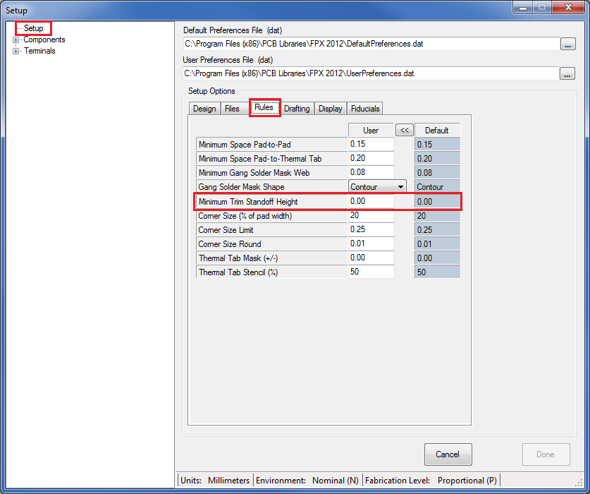 IPC just told us to turn the value off, they did not tell us to remove the feature. |
|
|
|
|
tphil
New User
Joined: 28 Jan 2013 Status: Offline Points: 2 |
Post Options
Thanks(0)
Quote Reply
Posted: 07 Feb 2013 at 8:42am |
|
I am aware that the feature is still there, but off by default. I was more interested to know if there if anybody has ever commented about solder joint reliability due to trimmed lands. Thanks for the reply.
|
|
|
|
|
Tom H
Admin Group
Joined: 05 Jan 2012 Location: San Diego, CA Status: Offline Points: 5716 |
Post Options
Thanks(0)
Quote Reply
Posted: 07 Feb 2013 at 8:53am |
|
No one has commented on this issue one way or the other and this issue is limited to Gull Wing lead components.
IPC's clarification is that the component leads are placed on top of 6 mils (0.15 mm) of paste mask during the pick & place assembly process. When the PCB goes through the oven, the component leads settle into the solder paste between 2 - 3 mils (0.05 mm - 0.75 mm) and if the component body comes in contact with the solder, it natural tendancy is to push the solder toward the Heel of the component lead and never shorts out between the leads under the component package. IPC's concern is that 70% the solder joint strength is in the Heel of the Gull Wing Lead and when you trim the Heel of the pad you effectively remove Heel solder and therefore reduce the Heel solder joint stength. |
|
|
|
|
Post Reply
|
|
| Tweet |
| Forum Jump | Forum Permissions You cannot post new topics in this forum You cannot reply to topics in this forum You cannot delete your posts in this forum You cannot edit your posts in this forum You cannot create polls in this forum You cannot vote in polls in this forum |


 Topic Options