

|
|
Solder Mask On 0.40 Pitch QFN |
Post Reply 
|
| Author | |
ArtCym 
New User 
Joined: 25 May 2022 Status: Offline Points: 4 |
 Post Options Post Options
") Thanks(0) Thanks(0)
 Quote Reply Quote Reply
 Topic: Solder Mask On 0.40 Pitch QFN Topic: Solder Mask On 0.40 Pitch QFNPosted: 25 May 2022 at 4:59am |
|
Hello,
I am working on a footprint for a QFN package (component MPN is ICM-20948) which has 0.4mm pitch and I'm not sure how to design the solder mask for this footprint. I saw some examples online where for QFNs of 400um pitch it was advised to use solder mask trench around the pads since it might be hard for the manufacturer to place solder mask between pads (minimum webbing of 100um in my case). Still, I would like to have solder mask between pads to help avoid solder bridges and I thought that I could use the nominal lead width instead of the maximum lead width to use for my footprint. I will use 50um solder mask clearance in my design. My idea is to use the nominal pad width (200um) + 2x50um of solder mask clearance leaving me with 100um for the solder mask webbing. My question is if it is too risky to use the nominal width of 200um instead of the maximum 250um but have the benefit of solder mask between pads? 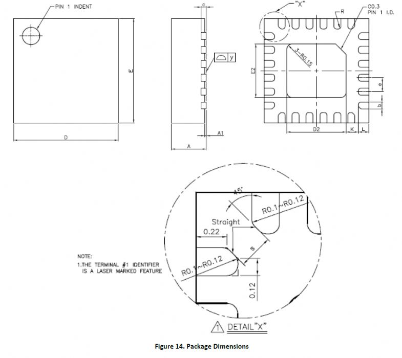 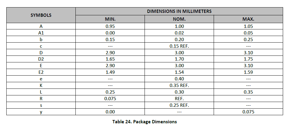 |
|
 |
|
|
|
|
Tom H
Admin Group 

Joined: 05 Jan 2012 Location: San Diego, CA Status: Offline Points: 5716 |
Post Options
Thanks(0)
Quote Reply
Posted: 25 May 2022 at 9:34am |
|
The Fabrication shop will automatically Gang Mask the entire row of pads on all 0.40 mm pitch packages.
|
|
|
|
|
feynman
Active User 
Joined: 06 Feb 2020 Status: Offline Points: 12 |
Post Options
Thanks(0)
Quote Reply
Posted: 27 May 2022 at 2:10pm |
|
You could simply make the solder mask openings 1:1 land size and leave the manufacturer the option for resizing according to their capabilities (in your fabrication notes). If they say they can do this you might want to explicitly call out in your final data to not gang mask, nevertheless. Because sometimes manufacturers can, but don't want to :) If they need more clearance than 50 um for the solder mask they will very likely Gang Mask it like Tom said. |
|
|
|
|
Post Reply
|
|
| Tweet |
| Forum Jump | Forum Permissions You cannot post new topics in this forum You cannot reply to topics in this forum You cannot delete your posts in this forum You cannot edit your posts in this forum You cannot create polls in this forum You cannot vote in polls in this forum |


 Topic Options