|
|
IPC-2221 & 2222 and Through-hole Pad Stacks |
Post Reply 
|
| Author | |
Tom H 
Admin Group 

Joined: 05 Jan 2012 Location: San Diego, CA Status: Offline Points: 5716 |
 Post Options Post Options
") Thanks(0) Thanks(0)
 Quote Reply Quote Reply
 Topic: IPC-2221 & 2222 and Through-hole Pad Stacks Topic: IPC-2221 & 2222 and Through-hole Pad StacksPosted: 24 Dec 2019 at 12:39pm |
|
The leading document for PCB fabrication is IPC-A-610. IPC-610
is used by most PCB fabrication shops to manufacture PCB’s for their customers
end-use, which are broken up into 3 Classes, 1, 2 or 3. CLASS 1 –
General Electronic Products Includes products suitable for applications where the major
requirement is function of the completed assembly. Toys CLASS 2 –
Dedicated Service Electronic Products Includes products where continued performance and extended
life is required, and for which uninterrupted service is desired but not
critical. Typically, the end-use environment would not cause failures.
Computers & Phones CLASS 3 –
High Performance Electronic Products Includes products where continued high performance or
performance-on-demand is critical, equipment downtime cannot be tolerated,
end-use environment may be uncommonly harsh, and the equipment must function
when required, such as life support or other critical systems. Military &
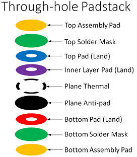
Medical This affects the CAD library Through-hole packages due to
the pad stack construction must meet or beat the IPC-610 rules for Annular
Rings, Plane Clearance, Inner Layer Pads, Thermal Relief Patterns as shown
below.
There are not many IPC-610 Fabrication rules for Surface
Mount Technology. Minimum pad to pad & solder mask swell for registration
might apply. But the pad size and spacing are most important for the Assembly
process for component attachment guidelines identified in the J-STD-001
standard. When defining a pad stack, you first must define the hole
size. This is done by taking the maximum lead diameter for round leads and the hypotenuse
of a rectangle shape lead. IPC considers that both round and rectangle leads
are the same, but PCB Libraries, Inc. believes that the round terminal lead
consumes more volume in the hole than a rectangle lead and therefore the hole
over round lead should be larger than hole over rectangle lead. Library Expert
allows the user to change both values independently. The Library Expert
Preference default values are Round Lead + 0.20 = Hole Size and Rectangular
lead + 0.15 = Hole Size. However, IPC-2222 has a table that is inclusive and
calculates the hole size based on Density Levels. See image below. 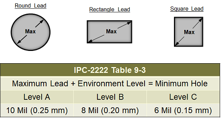 Once the Hole Size is established, the main point for pad
size calculation in the IPC-2221 standard is the minimum annular ring of the
plated through-hole pad stack after fabrication tolerances are applied. Here is
an image of the minimum annular ring.  There are 2 fabrication tolerances that must be accounted
for. The first and most obvious one is the hole size tolerance that is in the
drill chart on the fabrication drawing. The typical hole size tolerance for a
through-hole terminal lead is +/- 0.075 mm (3 mils) and vias are + 0/- Hole
Size. If the minimum annular ring for an external plated through-hole is 0.05
mm (2 mils) and the hole size tolerance is 0.075 mm, the pad size annular ring
must be 0.125 mm or a pad size of 0.25 mm over the hole size. The second tolerance that needs to be applied to calculate
the pad size is the layer to layer registration. This is typically held to
0.075 (3 mils) and only occurs when the layer count is greater than 4 layers. A
10 – 20 layer PCB could have layer to layer registration issues in every
direction on the inner layers. The minimum annular ring on the inner layers is
0.025 mm. For Class 3 boards that are 10 or more layers, the maximum layer to
layer registration should be held to +/- 0.05 mm. Also, the hole tolerance
should be set to +/- 0.05. Let’s make it simple. 0.025 minimum annular ring + 0.05
layer to layer registration + 0.025 hole tolerance = 0.10 annular ring or the
pad size = 0.20 over the hole size. But if the fabrication shop cannot hold the
layer to layer registration to 0.05 mm and requires 0.075 mm, then the minimum
pad size would be 0.25 mm over the hole. All of these values can be set in the Library Expert
software Preferences to ensure that your through-hole calculations meet or beat
your fabrication tolerance allowances.  The via hole quantity typically out numbers the terminal
lead holes and PCB designers want to make the via annular ring the minimum
value per the manufacturing Class that they must meet. Since there is no
terminal leads in a via hole, the hole size tolerance can be + 0/- Hole Size.
Allow the fabrication process to plate the via holes closed. If an inner layer
shifts 0.075 in any direction, the annular ring is affected. See the image
below. 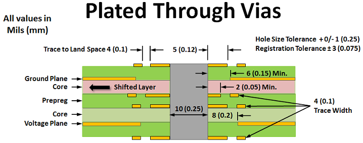 Another important pad stack calculation is the plane
anti-pad. Most fabrication shops require a minimum annular ring of 0.35 mm (15
mil) over the hole size. Making the plane anti-pad annular ring smaller could
cause the drill hole to be too close to the copper plane and making it larger
removes important plane copper that carries the signal return path for
transmission lines. Ideally, the plane anti-pad would be smaller than the pad
size + the electrical clearance. The electrical clearance is the trace to pad
spacing rule. All traces on all layers should be over a copper plane and not
intrude into the anti-pad area. Therefore, make the anti-pad large enough to
manufacture but small enough to maintain signal integrity. Note: The OD of the plane Thermal Relief is the same
diameter as the plane Anti-pad.  Incremental pad sizes are important for a couple reasons. Small
through-hole components have small terminal lead diameters that require smaller
hole sizes. Small packages are normally light in weight and they don’t carry
much current. Parts that require higher currents need larger terminal lead
diameters. High current parts generate more heat and are heavier in weight.
These features require a more robust annular ring that will allow more solder
to hold the part in place and to handle the heat transfer. The Library Expert
software program uses a default multiplier of 1.5 X hole size for the pad size
calculation. See the image above for the pad size calculation with a 1.0 mm
hole verses a 2.0 mm hole. The annular ring doubles in size. All of the pad stack calculation values in the Library
Expert software program come default with the best-known industry practices,
but they are all user definable to ensure that your plated through-hole
calculations meet or beat your corporate or customer standards. |
|
 |
|
|
|
|
AndrasP91
New User 
Joined: 20 Jul 2020 Status: Offline Points: 1 |
Post Options
Thanks(0)
Quote Reply
Posted: 20 Jul 2020 at 4:48am |
|
Hi there,
Thank you for the info!
|
|
|
|
|
npassey
Active User 
Joined: 16 Jul 2012 Location: Spokane Status: Offline Points: 10 |
Post Options
Thanks(0)
Quote Reply
Posted: 11 Aug 2020 at 6:52pm |
|
Hello Tom,
This is great info about drilled holes and padstacks. Is there a standard or guidance for PCB slot size? What's the best way to take the dimensions of the tab that will be soldered in a PTH slot and calculate the width X length for the slot? Thanks, -Nathan
|
|
|
The nice thing about standards is that there are so many to choose from.
-Tennenbaum |
|
|
|
|
Tom H
Admin Group
Joined: 05 Jan 2012 Location: San Diego, CA Status: Offline Points: 5716 |
Post Options
Thanks(0)
Quote Reply
Posted: 11 Aug 2020 at 7:12pm |
|
Slotted holes require 2x annular ring due to the drill and drag process.
|
|
|
|
|
npassey
Active User
Joined: 16 Jul 2012 Location: Spokane Status: Offline Points: 10 |
Post Options
Thanks(0)
Quote Reply
Posted: 12 Aug 2020 at 7:58am |
|
Tom, that annular ring info sounds good.
But my question was not about the padstack for a slot. I'm talking about calculating the milled slot hole. We are using custom metal shields in various locations that will be soldered to the PCB. I have the dimensions of the tab, and I can create a slot that will fit, but I'm mostly estimating. Your discussion above about the hole size for round and rectangular pins made me think to post this question here. Should I just extend the definition for pins into long, rectangular tabs and use something like IPC-2222B Table 9-5 (Figure 9-3) to calculate the slot hole? Thanks,
|
|
|
The nice thing about standards is that there are so many to choose from.
-Tennenbaum |
|
|
|
|
Tom H
Admin Group
Joined: 05 Jan 2012 Location: San Diego, CA Status: Offline Points: 5716 |
Post Options
Thanks(0)
Quote Reply
Posted: 12 Aug 2020 at 8:03am |
|
What CAD tool do you use for PCB layout?
We have something interesting in development that will help you. |
|
|
|
|
npassey
Active User
Joined: 16 Jul 2012 Location: Spokane Status: Offline Points: 10 |
Post Options
Thanks(0)
Quote Reply
Posted: 12 Aug 2020 at 8:56am |
|
Xpedition.
thanks,
|
|
|
The nice thing about standards is that there are so many to choose from.
-Tennenbaum |
|
|
|
|
Tom H
Admin Group
Joined: 05 Jan 2012 Location: San Diego, CA Status: Offline Points: 5716 |
Post Options
Thanks(0)
Quote Reply
Posted: 12 Aug 2020 at 9:19am |
|
We have a free software program called "Library Expert Pro" that supports Xpedition & high quality 3D STEP.
In that free program is 144 Calculators for standard component packages for both Surface Mount and Through-hole families. There is also a Toolbox with a Pad Stack Calculator. You can either enter the terminal lead length width or the hole size length and width and it will calculate all the pad stack details. Download and install the free Library Expert Pro here (no license required) - |
|
|
|
|
npassey
Active User
Joined: 16 Jul 2012 Location: Spokane Status: Offline Points: 10 |
Post Options
Thanks(0)
Quote Reply
Posted: 17 Aug 2020 at 6:45am |
|
Hi Tom,
Thanks for this. I have that tool, and earlier, I went to the toolbox and tried the "Hole Size Calculator". For some reason I did not see the Padstack Calculator, which answers my question. Have a great day!
|
|
|
The nice thing about standards is that there are so many to choose from.
-Tennenbaum |
|
|
|
|
Post Reply
|
|
| Tweet |
| Forum Jump | Forum Permissions You cannot post new topics in this forum You cannot reply to topics in this forum You cannot delete your posts in this forum You cannot edit your posts in this forum You cannot create polls in this forum You cannot vote in polls in this forum |


 Topic Options