

|
|
Footprint For Solderable Jumper? |
Post Reply 
|
| Author | |
LaserAlex 
Active User 

Joined: 06 Jun 2012 Location: Seattle, WA Status: Offline Points: 27 |
 Post Options Post Options
") Thanks(0) Thanks(0)
 Quote Reply Quote Reply
 Topic: Footprint For Solderable Jumper? Topic: Footprint For Solderable Jumper?Posted: 13 Feb 2017 at 2:55pm |
|
Does anyone have experience generating good (or bad!) footprints for solderable jumpers? I'm looking to configure a circuit board with something like this:
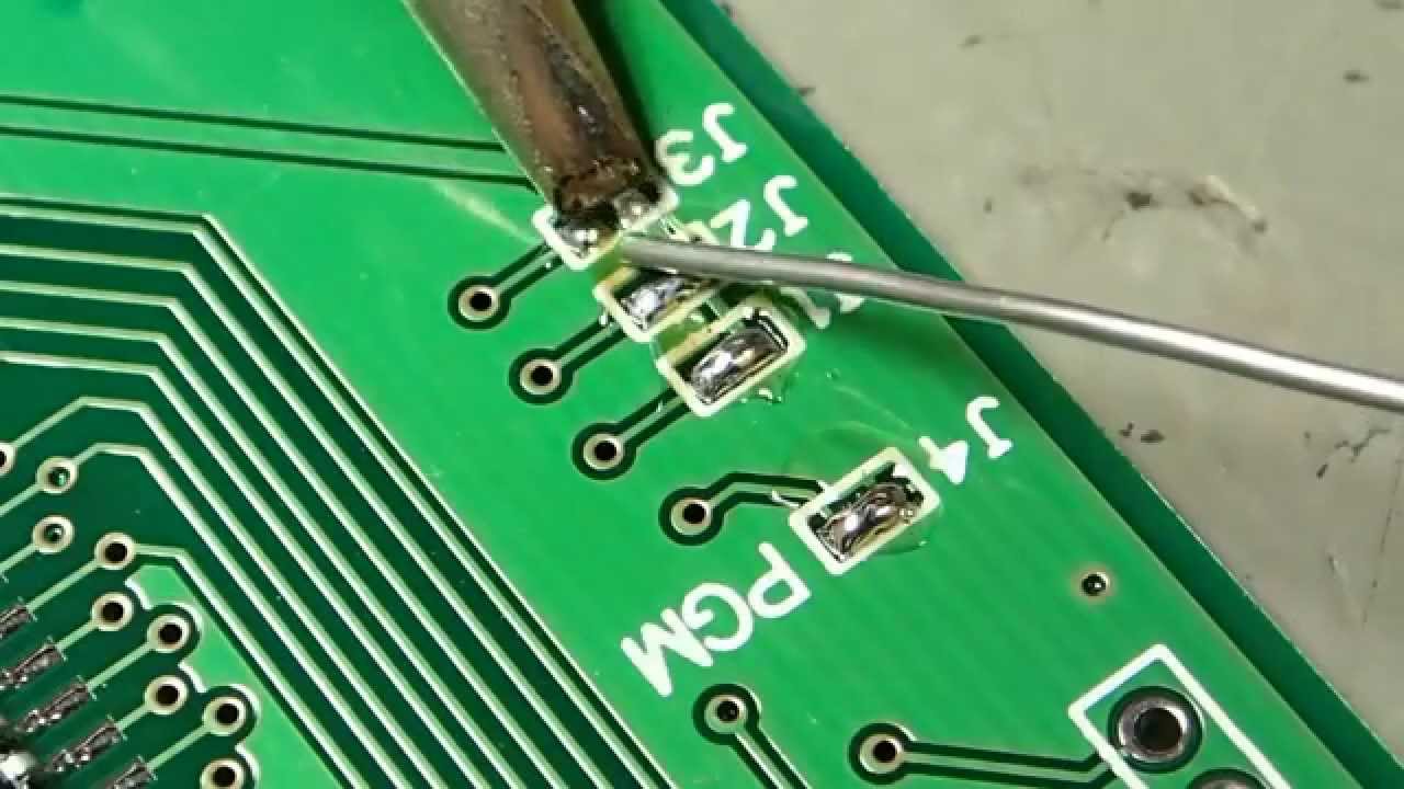 Or this: 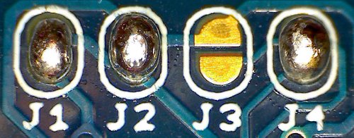 I want something that is easy and quick to connect, but also easy to desolder and clean up for reconfiguration. If it makes any difference, the intent is to use lead-free solder. Has anyone done this, with good or bad results? Can anyone provide pointers? Better yet, dimensions / configuration or even an Altium footprint for a "known-good" solder jumper? Thanks!
|
|
 |
|
|
|
|
Tom H
Admin Group 

Joined: 05 Jan 2012 Location: San Diego, CA Status: Offline Points: 5716 |
Post Options
Thanks(0)
Quote Reply
Posted: 13 Feb 2017 at 3:42pm |
|
Your picture is an OK example. There are just a couple rules -
Here are some alternate solder jumpers that work well -  |
|
|
|
|
LaserAlex
Active User
Joined: 06 Jun 2012 Location: Seattle, WA Status: Offline Points: 27 |
Post Options
Thanks(0)
Quote Reply
Posted: 13 Feb 2017 at 8:16pm |
|
Thank you for the quick response, Tom!
The options with the interdigitated contacts look like they would be very easy to short reliably, but I'm worried about the difficult of cleaning them up if the configuration needed to change. I'm sure solder wick and flux could clean them out, but I really want something easy to work with. Have you personally soldered and desoldered all of these? If you were tasked with reconfiguring a thousand of these jumpers, which would you prefer had been used on the board? Thanks! -Alex
|
|
|
|
|
Tom H
Admin Group
Joined: 05 Jan 2012 Location: San Diego, CA Status: Offline Points: 5716 |
Post Options
Thanks(0)
Quote Reply
Posted: 13 Feb 2017 at 8:51pm |
|
I'm an IPC CIT trainer for soldering and J-STD-001 solder joint acceptability and these patterns clean up really nice. Place a solder wick on the solder and apply the iron and the solder wick sucks up the solder and with a wire mesh touchup it should be clean to go. Old fashion pad with hole and wire is still a popular Jumper solution. Even a wire loop across 2 SMD pads with easy access to cut. No need to use a solder iron. |
|
|
|
|
LaserAlex
Active User
Joined: 06 Jun 2012 Location: Seattle, WA Status: Offline Points: 27 |
Post Options
Thanks(0)
Quote Reply
Posted: 13 Feb 2017 at 8:54pm |
|
Thanks, Tom. Great info!
|
|
|
|
|
MSM_KOPF
Advanced User 
Joined: 02 Feb 2015 Status: Offline Points: 53 |
Post Options
Thanks(0)
Quote Reply
Posted: 22 Feb 2019 at 5:34am |
|
How should such a footprint be named ? In my current footprint there are 2 pads each 0.5 x 1.0mm with a gap of 0.2mm between the 2 long sides. (02.mm Gap due to clearance requirements) There are versions of this footprint. 1. without any solder paste for an open solderable jumper 2. with solder paste over both pads and the gap between the pads for a close jumper after reflow A resistor would be something like "RESC1608X70" Is there any naming convention or recommendations for both footprints? |
|
|
|
|
Tom H
Admin Group
Joined: 05 Jan 2012 Location: San Diego, CA Status: Offline Points: 5716 |
Post Options
Thanks(0)
Quote Reply
Posted: 22 Feb 2019 at 8:46am |
|
If it's a Jumper I would use:
JUMP0510WP = Jumper 0.5 X 1.0 With Paste JUMP0510WOP = Jumper 0.5 X 1.0 With Out Paste You get the idea. |
|
|
|
|
DrewRu
New User 
Joined: 04 Oct 2019 Status: Offline Points: 1 |
Post Options
Thanks(0)
Quote Reply
Posted: 04 Oct 2019 at 7:22am |
|
Hi,
It is still common to represent this as an
optional 0 Ohm resistor and many designs still use a 0-Ohm SMD link; you
just have to remember to use the right footprint for the artwork if you
want to use a solder bridge.
|
|
|
|
|
Post Reply
|
|
| Tweet |
| Forum Jump | Forum Permissions You cannot post new topics in this forum You cannot reply to topics in this forum You cannot delete your posts in this forum You cannot edit your posts in this forum You cannot create polls in this forum You cannot vote in polls in this forum |


 Topic Options