

|
|
Requesting symbols and footprints for HX711... |
Post Reply 
|
| Author | |
Charu123 
New User 
Joined: 20 Jun 2020 Status: Offline Points: 2 |
 Post Options Post Options
") Thanks(0) Thanks(0)
 Quote Reply Quote Reply
 Topic: Requesting symbols and footprints for HX711... Topic: Requesting symbols and footprints for HX711...Posted: 21 Jun 2020 at 2:06am |
|
Hello All,
I am looking for a footprint for the HX711 Loadcell Amplifier Module 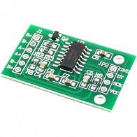 /weighing sensor.I am not very good at drawing a footprint. Would anyone know where i could find one ? /weighing sensor.I am not very good at drawing a footprint. Would anyone know where i could find one ?I already reffer footprint on snapeda of hx711(https://www.snapeda.com/parts/SEN-13879/SparkFun%20Electronics/view-part/?ref=search&t=hx711).But some difference of pins are in between what i need module and what i got.So do i edit that footprint or what to do please let me know .I am new to this software so,looking forward to get proper solution for it. |
|
 |
|
|
|
|
Tom H
Admin Group 

Joined: 05 Jan 2012 Location: San Diego, CA Status: Offline Points: 5716 |
Post Options
Thanks(0)
Quote Reply
Posted: 22 Sep 2020 at 9:41am |
|
The footprint you are looking for is a simple 16-pin 1.27 mm pitch SOIC.
You can insert the package dimensions and build the part out to 25 CAD tools and 3D STEP using the Free V2020 Library Expert Pro. |
|
|
|
|
Post Reply
|
|
| Tweet |
| Forum Jump | Forum Permissions You cannot post new topics in this forum You cannot reply to topics in this forum You cannot delete your posts in this forum You cannot edit your posts in this forum You cannot create polls in this forum You cannot vote in polls in this forum |


 Topic Options