

|
|
JEDEC MO-240 AA ? |
Post Reply 
|
| Author | |
Matthew Lamkin 
Advanced User 
Joined: 02 Oct 2012 Status: Offline Points: 284 |
 Post Options Post Options
") Thanks(0) Thanks(0)
 Quote Reply Quote Reply
 Topic: JEDEC MO-240 AA ? Topic: JEDEC MO-240 AA ?Posted: 23 Jan 2015 at 5:30am |
|
HI, for the JEDEC MO-240 Var AA for a Fairchild FDMS7650 etc.
This is like an SO8 with a big heat pad inthe middle where it is connected to 4 of the outer pads. In this part it has 4 common pads for the "Drain".  If the component layout for this has the big centre pad and the 4 drain pads all within the same sodler resist clearance, so that there is no sodler resist between the 4 drain pads and the heat slug - when reflow soldering would there be a tendency for the solder from the 4 pads to wick back onto the heat slug leaving them with poor connection? The manufacturers recommended footprint is: 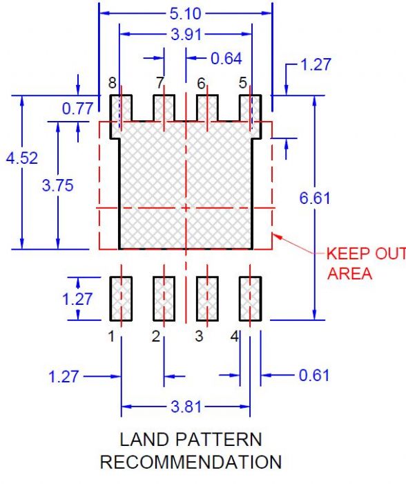 Now given that they are bonded to the same heat slug on the component I'm not sure it really matters. In the past I usually make this with a big rectangular pad for the slug with its own solder resist and 4 separate pads for the drain connections. This gives each one their own solder resist shape & hence a gap between the 4 & the slug. So I am wondering whatIPC7351 says about it? what others would do about the above and where to start in the wizard for this - what SMT family to choose to start etc? Cheers, Matthew |
|
 |
|

|
|
|
|
|
jameshead
Expert User 

Joined: 20 Mar 2012 Location: Oxfordshire, UK Status: Offline Points: 576 |
Post Options
Thanks(0)
Quote Reply
Posted: 23 Jan 2015 at 6:13am |
|
We use a similar packaged device, Texas Instruments CSD16340Q3. We use the manufacturer's recommended land pattern but created on PCB Libraries.
|
|
|
|
|
Tom H
Admin Group 

Joined: 05 Jan 2012 Location: San Diego, CA Status: Offline Points: 6075 |
Post Options
Thanks(0)
Quote Reply
Posted: 23 Jan 2015 at 8:25am |
|
IPC does not have any guidance on non-standard component packages.
You should use the mfr. recommended pattern. This is a very easy part to create in FP Designer. In the Sample FPX that comes with Library Expert, look at these footprints -
|
|
|
|
|
Matthew Lamkin
Advanced User
Joined: 02 Oct 2012 Status: Offline Points: 284 |
Post Options
Thanks(0)
Quote Reply
Posted: 23 Jan 2015 at 8:29am |
|
What about my thoughts on the solder resist between the smaller & large pad?
When creating the component in FPX - what SMT family should I start with? P.S> I only have lite at the moment, the full version complained of a license problem that I have not got around to sorting yet. Cheers, Matthew |
|
|
|
|
Tom H
Admin Group
Joined: 05 Jan 2012 Location: San Diego, CA Status: Offline Points: 6075 |
Post Options
Thanks(0)
Quote Reply
Posted: 23 Jan 2015 at 8:41am |
|
Nick will help you with your license issue.
The past mask of the Thermal Pad should not touch the paste mask of the smaller pads. We can relocate the Thermal Pad Paste Mask internally and then output a XML FPX file that can be opened in Library Expert. Do not co-minge XML FPX with ASCII FPX as they are 2 different formats. I would highly recommend to use Parts on Demand and Request a Part - www.pcblibraries.com/pod Here is a XML FPX sample of the Thermal Pad Paste Mask moved away from the smaller pads - |
|
|
|
|
Matthew Lamkin
Advanced User
Joined: 02 Oct 2012 Status: Offline Points: 284 |
Post Options
Thanks(0)
Quote Reply
Posted: 24 Jan 2015 at 9:13am |
|
I'm away this week so will not be able to sort out any license problems.
Tom, Solder resist is not solder paste :) Bit IMO the same should apply to the resist as the paste, that way the thermal pad paste does not get anywhere the outer pads irrespective of whatever the copper layout it. |
|
|
|
|
Tom H
Admin Group
Joined: 05 Jan 2012 Location: San Diego, CA Status: Offline Points: 6075 |
Post Options
Thanks(0)
Quote Reply
Posted: 24 Jan 2015 at 10:07am |
|
The Solder Mask is removed from all metal surfaces. Full Paste Mask coverage is applied to the Lead Terminals and 50% reduction on the Thermal Pad. There doesn't seem to be any guidance from the component mfr. (CM) on this subject of "Solder Dam" that would prevent the Lead Terminal solder from wandering onto the Thermal Pad during reflow. I would think that the Solder Mask would have a break line to prevent that. The CM's should have better drawings and illustrations. I'll bring this subject up at the next IPC-7351 executive committee meeting at IPC APEX on Wednesday February 25. But I need to gather information from the industry and assembly shops to present it to the committee. |
|
|
|
|
Matthew Lamkin
Advanced User
Joined: 02 Oct 2012 Status: Offline Points: 284 |
Post Options
Thanks(0)
Quote Reply
Posted: 25 Jan 2015 at 3:24pm |
|
Cheers Tom.
It probably won't actually make any difference as the 4 drain pins are connected to the tab but IMO it will lead to poor looking joints on those pins which no one likes to see. :) |
|
|
|
|
Post Reply
|
|
| Tweet |
| Forum Jump | Forum Permissions You cannot post new topics in this forum You cannot reply to topics in this forum You cannot delete your posts in this forum You cannot edit your posts in this forum You cannot create polls in this forum You cannot vote in polls in this forum |


 Topic Options