

|
|
No Silk on DPAK ?? |
Post Reply 
|
| Author | |
DickMS 
Active User 

Joined: 04 Jan 2014 Location: Seattle, WA, US Status: Offline Points: 33 |
 Post Options Post Options
") Thanks(0) Thanks(0)
 Quote Reply Quote Reply
 Topic: No Silk on DPAK ?? Topic: No Silk on DPAK ??Posted: 23 Jan 2014 at 8:56pm |
|
I just finished making a footprint for an Alpha-Omega FET in a DPAK package. While I selected the package to start from SM.fpx, I specified the manufacturer's recommended spacing on the final pads. FPX then told me it couldn't output any Silkscreen because the geometry was too small!!! I've included a new library with the part in it, for your debugging.... Any help would be appreciated!
-- Dick 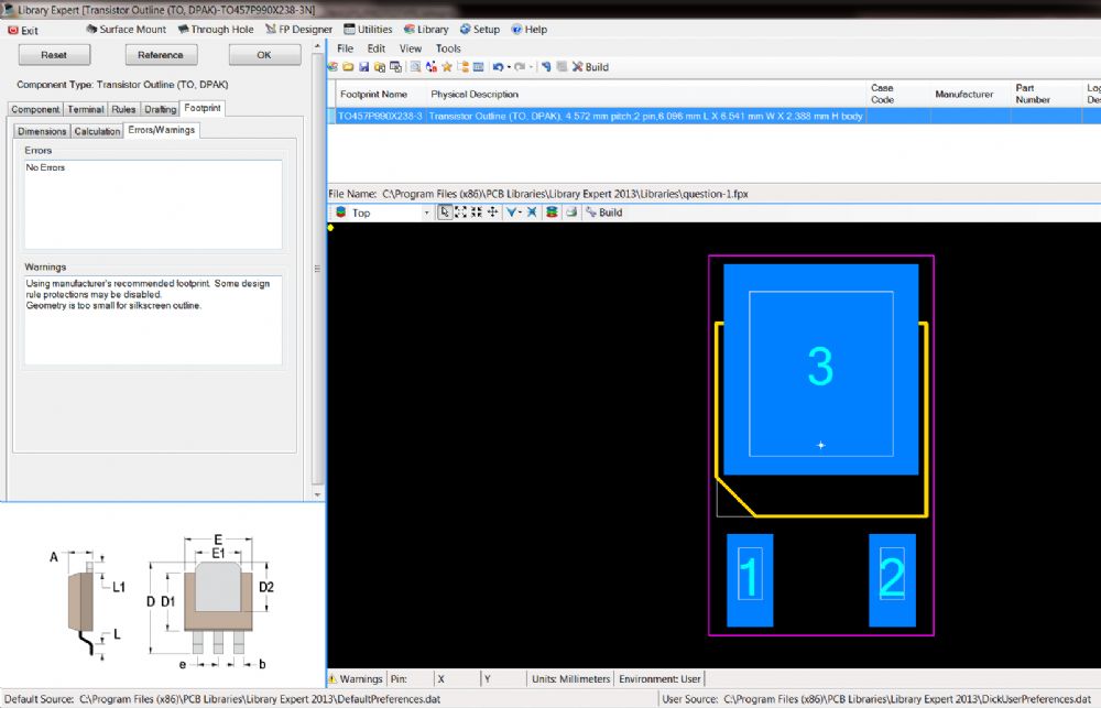 |
|
 |
|

|
|
|
|
|
Jeff.M
Admin Group 

Joined: 16 May 2012 Location: San Diego Status: Offline Points: 501 |
Post Options
Thanks(0)
Quote Reply
Posted: 24 Jan 2014 at 9:40am |
|
The geometry is too small. According to the rules for silkscreen clearance and line widths there isn't enough space between the pad and the outside body dimension to place any of the six possible outline shapes.
Obviously it could be drawn oversize, i.e. beyond the size of the body, but we don't currently provide for that because it would misrepresent the body.
|
|
|
|
|
DickMS
Active User
Joined: 04 Jan 2014 Location: Seattle, WA, US Status: Offline Points: 33 |
Post Options
Thanks(0)
Quote Reply
Posted: 24 Jan 2014 at 9:49am |
|
Sorry - if you can draw silk on a resistor that's 0402, then I see no possible reason for not drawing on a transistor that's 100 times as big - maybe your pattern in SM is not specified correctly?
|
|
|
|
|
Tom H
Admin Group

Joined: 05 Jan 2012 Location: San Diego, CA Status: Offline Points: 6074 |
Post Options
Thanks(0)
Quote Reply
Posted: 24 Jan 2014 at 12:46pm |
|
This does seem a bit strange. Can you send me the FPX file? You also know that you can change the Silkscreen to Pad Clearance and the Silkscreen Line Width and the Library Expert will eventually drop in a silkscreen. But I'm really curious on why you're getting the message "Component Too Small for Silkscreen Outline". |
|
|
|
|
DickMS
Active User
Joined: 04 Jan 2014 Location: Seattle, WA, US Status: Offline Points: 33 |
Post Options
Thanks(0)
Quote Reply
Posted: 24 Jan 2014 at 1:05pm |
|
uploads/8170/question-1.zip
Thanks, Tom - your programmer seemed a bit unfamiliar with the needs of layout folk - anyone who says that his own database violates his own rules, and I don't need a silkscreen anyway is a bit behind the curve on customer service, and real users' needs. Here's the zip file with the picture and the fpx in it... Thanks for taking this over! (and yes, I knew how to change the spacing rules - but that shouldn't be necessary on something so common, pulled from your main SM library - if they can be made to work with a flea-sized resistor, then they should be able to work with something as big as a DPAK. I suspect something in the library data is out of whack and needs some attention.) --Dick
|
|
|
|
|
Post Reply
|
|
| Tweet |
| Forum Jump | Forum Permissions You cannot post new topics in this forum You cannot reply to topics in this forum You cannot delete your posts in this forum You cannot edit your posts in this forum You cannot create polls in this forum You cannot vote in polls in this forum |


 Topic Options