

|
|
IPC-7351C |
Post Reply 
|
| Author | |
bnoel 
Active User 

Joined: 14 Mar 2014 Location: Western NY Status: Offline Points: 14 |
 Post Options Post Options
") Thanks(0) Thanks(0)
 Quote Reply Quote Reply
 Topic: IPC-7351C Topic: IPC-7351CPosted: 10 Feb 2023 at 4:47am |
|
Hello - We've been using the IPC-7351 LP Calculator V10.3 in viewer mode to determine our land patterns and then create our footprints in our tools (OrCAD and Altium) using the results from the calculator. I believe that this calculator is based on IPC-7351B. We also have the Footprint Expert Pro (2021.04) calculator in viewer mode. I believe this calculator is based on the unreleased revC version of IPC-7351.
We have also been receiving feedback from our assembly houses that the footprints for small discrete packages (0402, 0201 in particular) is not ideal and is causing manufacturing issues. In most cases the assembly houses are recommending smaller pad sizes to mitigate the issue. I have run comparisons between the 2 calculators and the newer Footprint Expert Pro Calculator provides significantly smaller pad sizes and overall geometries than the older LP Calculator. Is it possible that with the upcoming revC release of 7351 it has been recognized that changes needed to be made to the solder calculations for newer assembly processes and these new calculations have been incorporated into the new calculator? If this is correct how safe to you feel it would be to use the new calculator going forward without revC being officially released? Thank you in advance for your guidance in this matter.
|
|
 |
|

|
|
|
|
|
Tom H
Admin Group 

Joined: 05 Jan 2012 Location: San Diego, CA Status: Offline Points: 6074 |
Post Options
Thanks(0)
Quote Reply
Posted: 10 Feb 2023 at 9:33am |
|
The V23.03 Footprint Expert follows the IPC J-STD-001 Standard for Solder Joint Goals. Every chip size has unique Toe, Heel and Side for all 3 Density Levels for Least, Nominal and Most.
IPC-7351C was renamed to IPC-7352 and includes guidelines and Naming Convention for through-hole packages. The IPC-7351B was released in early 2010. The 0201 package wasn't released yet. And the IPC-7351B is not an incremental solder joint solution where every chip size has it's own solder joint goals. Here are the V23.03 Footprint Expert Solder Joint Goals. The Toe goal is the most important. I assume that you are using something different. 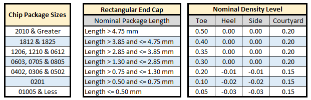 |
|
|
|
|
bnoel
Active User
Joined: 14 Mar 2014 Location: Western NY Status: Offline Points: 14 |
Post Options
Thanks(0)
Quote Reply
Posted: 10 Feb 2023 at 11:11am |
|
We have been using both LP Land calculator v10.3 and Footprint Expert 2021 Pro "out of the box" so whatever default settings are that's what we've been using. I have installed 23 Pro but have not been able to get it to work in viewer mode. It keeps closing even though I receive a message that says it will continue in viewer mode only.
I calculated geometries for an 0402 cap using both 10.3 and Expert 2021 and I got substantial differences in pad geometries even though I was set to nominal and/or least in both. Is that what I should be seeing? Can you help me get 23 Pro going in viewer mode? I was going to compare results from it to 10.3 and 2021 Pro.
|
|
|
|
|
Tom H
Admin Group
Joined: 05 Jan 2012 Location: San Diego, CA Status: Offline Points: 6074 |
Post Options
Thanks(0)
Quote Reply
Posted: 10 Feb 2023 at 11:19am |
|
Viewer Mode cannot calculate footprints. We don't know how you're using a Viewer in a productive way.
|
|
|
|
|
feynman
Active User
Joined: 06 Feb 2020 Status: Offline Points: 18 |
Post Options
Thanks(0)
Quote Reply
Posted: 10 Feb 2023 at 11:24am |
|
For chip components size 0603 and smaller I would always ask your assembler for a land pattern that works best. Or at least use the manufacturer's recommendation. I've received feedback from assemblers as well that chip component land patterns calculated with FPX don't work very well. Feedback always was that the pads were too big.
|
|
|
|
|
Tom H
Admin Group
Joined: 05 Jan 2012 Location: San Diego, CA Status: Offline Points: 6074 |
Post Options
Thanks(0)
Quote Reply
Posted: 10 Feb 2023 at 11:45am |
|
The Side and Heel goals are 0.00 so the only significant value is the Toe.
The IPC J-STD-001 Standard says that the Chip Toe goal should be at least 25% of the package height or 0.50 mm, whichever is less. |
|
|
|
|
feynman
Active User
Joined: 06 Feb 2020 Status: Offline Points: 18 |
Post Options
Thanks(0)
Quote Reply
Posted: 11 Feb 2023 at 6:37am |
|
Yes, it appears to me that the toe calculated with "Nominal" material condition tends to be too big (at least for 0603 and smaller and especially for capacitors). A toe calculated with "Least" material condition is much closer to what assemblers are recommending. |
|
|
|
|
Post Reply
|
|
| Tweet |
| Forum Jump | Forum Permissions You cannot post new topics in this forum You cannot reply to topics in this forum You cannot delete your posts in this forum You cannot edit your posts in this forum You cannot create polls in this forum You cannot vote in polls in this forum |


 Topic Options