

|
|
Terminal Dimensions for Non-Standard Packages |
Post Reply 
|
| Author | |
mohamedjubair.k 
Active User 
Joined: 05 Sep 2022 Status: Offline Points: 26 |
 Post Options Post Options
") Thanks(1) Thanks(1)
 Quote Reply Quote Reply
 Topic: Terminal Dimensions for Non-Standard Packages Topic: Terminal Dimensions for Non-Standard PackagesPosted: 05 Sep 2022 at 5:51am |
|
Hi Everyone,
Please anyone guide me, how to get this unknown dimension. Generally for all SMD connectors, lead length value is not mentioned in datasheet. Is there any other way, how to obtain this missing dimension other than 3D model. Please help me out of this riddle. The below image is a sample. 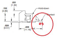 |
|
 |
|

|
|
|
|
|
Tom H
Admin Group 

Joined: 05 Jan 2012 Location: San Diego, CA Status: Offline Points: 6074 |
Post Options
Thanks(0)
Quote Reply
Posted: 05 Sep 2022 at 8:02am |
|
You must use the manufacturer recommended pattern to create your footprint.
|
|
|
|
|
mohamedjubair.k
Active User
Joined: 05 Sep 2022 Status: Offline Points: 26 |
Post Options
Thanks(0)
Quote Reply
Posted: 05 Sep 2022 at 9:04am |
|
Hi Tom,
Thank you for your reply. Actually I need the mechanical dimensions of the lead to draw VPL Packages . I couldn't find this dimension alone in most of the connector datasheets. Why they are not mentioning length of the lead. Is there any way to find this other than 3D model. Without this I couldn't draw VPL.
|
|
|
|
|
Tom H
Admin Group
Joined: 05 Jan 2012 Location: San Diego, CA Status: Offline Points: 6074 |
Post Options
Thanks(0)
Quote Reply
Posted: 05 Sep 2022 at 9:10am |
|
I could investigate but I need the mfr. name and part number.
|
|
|
|
|
mohamedjubair.k
Active User
Joined: 05 Sep 2022 Status: Offline Points: 26 |
Post Options
Thanks(1)
Quote Reply
Posted: 05 Sep 2022 at 9:45am |
|
Hi Tom,
Part number is 2-1445057-2 and from TE connectivity. This is for example only. Mostly for all connectors which has "L" lead form this dimension is not mentioned. For creating VPL we will use mechanical dimensions only.
|
|
|
|
|
Tom H
Admin Group
Joined: 05 Jan 2012 Location: San Diego, CA Status: Offline Points: 6074 |
Post Options
Thanks(0)
Quote Reply
Posted: 05 Sep 2022 at 9:53am |
|
It is true that most surface mount connector manufacturer's do not provide the terminal lead dimensions.
This is why we must use the mfr. recommended pattern for the PCB solder pattern. The only thing you can do is download the 3D STEP model and open it in a 3D model program like SolidWorks and use the measure feature. |
|
|
|
|
mohamedjubair.k
Active User
Joined: 05 Sep 2022 Status: Offline Points: 26 |
Post Options
Thanks(1)
Quote Reply
Posted: 05 Sep 2022 at 6:45pm |
|
Thank you Tom.
|
|
|
|
|
mohamedjubair.k
Active User
Joined: 05 Sep 2022 Status: Offline Points: 26 |
Post Options
Thanks(0)
Quote Reply
Posted: 11 Oct 2022 at 12:48am |
|
Hi Tom,
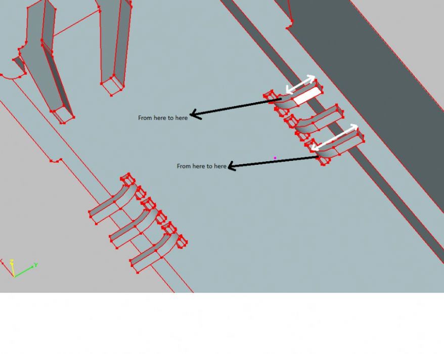
This is a DDR4 DIMM socket. physical pin dimension is not mentioned in component drawing. As we discussed i downloaded a 3D step file. Now my question is from where to where the pin length measurement will be. I marked 2 way in attached image. Because, Design rule checks will be based on physical dimensions of the pin. We will inspect toe and heel joint value for a lead based upon IPC and we will confirm the CAD footprint. So this pin length value is much important. Please educate me regarding this.
 |
|
|
|
|
Tom H
Admin Group
Joined: 05 Jan 2012 Location: San Diego, CA Status: Offline Points: 6074 |
Post Options
Thanks(0)
Quote Reply
Posted: 11 Oct 2022 at 9:44am |
|
Make the "Toe" value the same dimension as the terminal lead thickness.
Make the Heel value 0.35 mm and the side goal 0.05 mm. The terminal length is the white area that you define in your picture. The Pad Length is the Terminal Length + Toe + Heel. The pad width is the Terminal width + 0.10 mm |
|
|
|
|
mohamedjubair.k
Active User
Joined: 05 Sep 2022 Status: Offline Points: 26 |
Post Options
Thanks(0)
Quote Reply
Posted: 12 Oct 2022 at 7:04am |
|
Thank you, Tom.
|
|
|
|
|
Post Reply
|
|
| Tweet |
| Forum Jump | Forum Permissions You cannot post new topics in this forum You cannot reply to topics in this forum You cannot delete your posts in this forum You cannot edit your posts in this forum You cannot create polls in this forum You cannot vote in polls in this forum |


 Topic Options