
 |

|
Courtyard Size Versus Padstacks |
Post Reply 
|
Page 12> |
| Author | |
dwaltoneng 
Advanced User 
Joined: 02 Mar 2013 Location: Australia Status: Offline Points: 193 |
 Post Options Post Options
 Thanks(1) Thanks(1)
 Quote Quote  Reply Reply
 Topic: Courtyard Size Versus Padstacks Topic: Courtyard Size Versus PadstacksPosted: 13 Jun 2013 at 7:08pm |
|
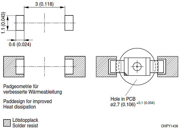
I was trying to use the FP Designer to create this component LG M47K http://catalog.osram-os.com/jsp/download.jsp?name=LG_M47K_Pb_free.pdf&url=/media/_en/Graphics/00042011_0.pdf
If I create a pad for the surface mount pins and a through hole pad for the component body, when I place the surface mount pads, the courtyard is expanded as if I had placed the large through hole pad instead of the smaller surface mount pads. I end up with a very long courtyard for the component. If I create a pad for the surface mount pins, place the surface mount pins and then create the through hole pad and place it, the courtyard appears to be sized correctly. I am using PCB Library Expert version: 2013.03 |
|
 |
|

|
|
 |
|
Tom H 
Admin Group 

Joined: 05 Jan 2012 Location: San Diego, CA Status: Offline Points: 6029 |
 Post Options Post Options
 Thanks(0) Thanks(0)
 Quote Quote  Reply Reply
 Posted: 13 Jun 2013 at 7:31pm Posted: 13 Jun 2013 at 7:31pm |
|
The Placement Courtyard and the Silkscreen Outline play tricks in the FP Designer that you have to get used to.
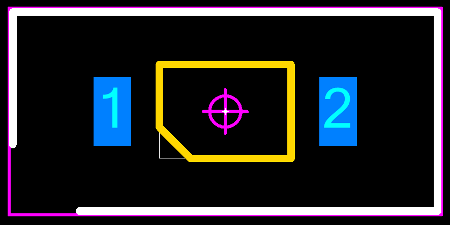
When you enter the component body dimensions, the silkscreen will be intially auto-generated using those dimensions and the courtyard excess will be adjusted per those numbers plus the oversize value you enter. Then when you place the pads and if they come near the silkscreen outline, the silkscreen outline will auto-adjust per your user preference rules for Pad to Silkscreen rule and move the silkscreen to obey the rule. However, the courtyard does not grow like the silkscreen. The courtyard will stay oversized to the same value as the original component body dimensions. So the pads push the silkscreen to obey your rules but the courtyard follows your component body dimensions. This was hard for me to understand at first because sometimes the courtyard will look weird or irregular spacing around the silkscreen due to the pad to silkscreen clearance rule. The Footprint you are trying to build is very interesting. The non-plated hole would be located at 0,0 and the 2 SMT pads are easy to place. When the "Parts on Demand" (POD) website opens, the FPX file for this part should be available to everyone in the industry so that only one person enters the dimensional data and everyone else can download the FPX file, import it and auto-generate the Footprint is any CAD tool format. And can you imagine millions of component mfr. part numbers available at your finger tips ready for download.  OSRAM_LGM47K Hyper-Bright Low Current LED |
|
 |
|
dwaltoneng 
Advanced User 
Joined: 02 Mar 2013 Location: Australia Status: Offline Points: 193 |
 Post Options Post Options
 Thanks(1) Thanks(1)
 Quote Quote  Reply Reply
 Posted: 13 Jun 2013 at 8:08pm Posted: 13 Jun 2013 at 8:08pm |
|
When I define the component body, the courtyard and silkscreen are both auto generated. When I add pads, both the courtyard and the silkscreen expand. Why does the amount the courtyard and silkscreen expand depend not only on the pads that have been placed, but also on the pad shapes that have been defined but not yet placed?
|
|
 |
|
Tom H 
Admin Group 

Joined: 05 Jan 2012 Location: San Diego, CA Status: Offline Points: 6029 |
 Post Options Post Options
 Thanks(0) Thanks(0)
 Quote Quote  Reply Reply
 Posted: 13 Jun 2013 at 8:15pm Posted: 13 Jun 2013 at 8:15pm |
|
I'm going to have Jeff answer this question from a programmers view point. So you'll have to wait until tomorrow for the answer. I hope you're coming to the SMCBA conference in Melbourne in September - Hope to see you there! |
|
 |
|
Jeff.M 
Admin Group 

Joined: 16 May 2012 Location: San Diego Status: Offline Points: 499 |
 Post Options Post Options
 Thanks(0) Thanks(0)
 Quote Quote  Reply Reply
 Posted: 14 Jun 2013 at 7:49am Posted: 14 Jun 2013 at 7:49am |
|
In the footprint designer the silkscreen can get pushed out to comply with silk-to-pad clearance rules.
When this happens the courtyard can also, but not necessarily always, get pushed out to keep the silkscreen inside the courtyard. If the shape is square or rectangular, this should only happen on a side where the violation occurs. If you can provide a screen image I may be able to explain further or a correction may be required in the software. |
|
 |
|
dwaltoneng 
Advanced User 
Joined: 02 Mar 2013 Location: Australia Status: Offline Points: 193 |
 Post Options Post Options
 Thanks(1) Thanks(1)
 Quote Quote  Reply Reply
 Posted: 14 Jun 2013 at 3:04pm Posted: 14 Jun 2013 at 3:04pm |
|
It turns out that it is the order that you define pads in that makes
the difference. If you define the surface mount pad first, when you
place the pad, the courtyard will be adjusted to fit that pad. If you
define the large through hole pad before the surface mount pad, when you
place the surface mount pad, the courtyard is adjusted as though you
placed the through hole pad.
Surface mount pad defined first -  Large through hole pad define first, but not placed  |
|
 |
|
dwaltoneng 
Advanced User 
Joined: 02 Mar 2013 Location: Australia Status: Offline Points: 193 |
 Post Options Post Options
 Thanks(1) Thanks(1)
 Quote Quote  Reply Reply
 Posted: 21 Jun 2013 at 4:30pm Posted: 21 Jun 2013 at 4:30pm |
|
Is this behavior expected?
|
|
 |
|
Jeff.M 
Admin Group 

Joined: 16 May 2012 Location: San Diego Status: Offline Points: 499 |
 Post Options Post Options
 Thanks(0) Thanks(0)
 Quote Quote  Reply Reply
 Posted: 24 Jun 2013 at 5:58pm Posted: 24 Jun 2013 at 5:58pm |
|
I'm having a hard time figuring out what the problem is here.
I don't see a hole in pictures provided for this part. The data sheet is incomplete in that it provides no body details and from what I can do in the way of trying to reproduce the report isn't exposing any problem. Plus the solder mask as defined is can not be created in the FP designer. Can you provide a more detailed explanation? We may need an on-line meeting. Thanks.
|
|
 |
|
dwaltoneng 
Advanced User 
Joined: 02 Mar 2013 Location: Australia Status: Offline Points: 193 |
 Post Options Post Options
 Thanks(1) Thanks(1)
 Quote Quote  Reply Reply
 Posted: 24 Jun 2013 at 7:16pm Posted: 24 Jun 2013 at 7:16pm |
Page 9 of the data sheet http://catalog.osram-os.com/jsp/download.jsp?name=LG_M47K_Pb_free.pdf&url=/media/_en/Graphics/00042011_0.pdf I quoted in my original post does provide body details. This part is a reverse mounted LED. The entire body of the part sits in a 2.7mm hole. Please try the following sequence: Define a rectangular body H=0.4 W=1.5 L=2.1 Define a 1.1 x 0.6 surface mount pad. Define a non plated through mounting pad with a 2.7mm hole. Place two of the surface mount pads at 3.6mm centers. Please reset and try the following sequence: Define a rectangular body H=0.4 W=1.5 L=2.1 Define a non plated through mounting pad with a 2.7mm hole. Define a 1.1 x 0.6 surface mount pad. Place two of the surface mount pads at 3.6mm centers. The previous two sequences yield different results, even though the through hole pad has not even been placed yet. |
|
 |
|
dwaltoneng 
Advanced User 
Joined: 02 Mar 2013 Location: Australia Status: Offline Points: 193 |
 Post Options Post Options
 Thanks(1) Thanks(1)
 Quote Quote  Reply Reply
 Posted: 02 Jul 2013 at 4:23pm Posted: 02 Jul 2013 at 4:23pm |
|
I just tried repeating the steps listed in the previous post, but this time I saved both of the results to a library. When the components were created, they looked like the screen shots in an earlier post, but when I retrieve them from the library, they both looked the same as the screen shot for "Surface mount pad defined first". This is possibly because the pad stack for the unused through hole pad has been discarded.
If I actually place the central hole, the problem remains. tst_3 sequence: Define a rectangular body H=0.4 W=1.5 L=2.1 Define a 1.1 x 0.6 surface mount pad. Define a non plated through mounting pad with a 2.7mm hole. Place the hole at 0,0. Place two of the surface mount pads at 3.6mm centers. tst_4 sequence: Define a rectangular body H=0.4 W=1.5 L=2.1 Define a non plated through mounting pad with a 2.7mm hole. Define a 1.1 x 0.6 surface mount pad. Place the hole at 0,0. Place two of the surface mount pads at 3.6mm centers. uploads/2945/courtyard_test.fpx shows the results of defining the component. |
|
 |
|
Post Reply 
|
Page 12> |
| Tweet |
| Forum Jump | Forum Permissions  You cannot post new topics in this forum You cannot reply to topics in this forum You cannot delete your posts in this forum You cannot edit your posts in this forum You cannot create polls in this forum You cannot vote in polls in this forum |