

|
|
Capacitor construction help |
Post Reply 
|
| Author | |
dramos 
Advanced User 
Joined: 18 Feb 2021 Status: Offline Points: 101 |
 Post Options Post Options
") Thanks(0) Thanks(0)
 Quote Reply Quote Reply
 Topic: Capacitor construction help Topic: Capacitor construction helpPosted: 14 Feb 2023 at 4:20am |
|
Hi to all,
I want to create a footprint for a TDK capacitor C2012X5R1V226M125AC. Reading the documentation I realized that the manufacturer does not mark the max and min size of the metallization. Instead of it, we have the value of the min metallization length and min length of the ceramic body of the part. 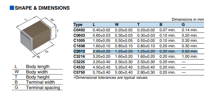 And here is my question, would be right to think that the metallization max length is equal to the length max of the part minus the in length of the ceramic body and divided by two? 2.20mm - 0.50mm =1.7mm / 2 = 0.85mm Therefore, the metallization size would be 0.2mm - 0.85mm Is normal to find the metallization length in that way (min metallization-min ceramic body)? Thanks to all for your help. David
|
|
 |
|

|
|
|
|
|
SDTKO
Active User 
Joined: 11 Dec 2019 Status: Offline Points: 31 |
Post Options
Thanks(0)
Quote Reply
Posted: 14 Feb 2023 at 5:21am |
|
That's what I would do as well. Maybe the manufacturer also has a recommended land pattern? It's a common thing for manufacturers to specify the min. ceramic body length. If you have requirements regarding creepage distances (e. g. medical), this dimension gives you directly what you need to know.
|
|
|
|
|
Tom H
Admin Group 

Joined: 05 Jan 2012 Location: San Diego, CA Status: Offline Points: 6075 |
Post Options
Thanks(0)
Quote Reply
Posted: 14 Feb 2023 at 9:15am |
|
When the manufacturer does not provide the adequate dimensional data, I always search for the mfr. recommended pattern and then insert dimensions until I come close to that pattern.
https://product.tdk.com/en/search/capacitor/ceramic/mlcc/info?part_no=C2012X5R1V226M125AC 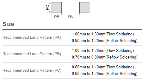 |
|
|
|
|
dramos
Advanced User
Joined: 18 Feb 2021 Status: Offline Points: 101 |
Post Options
Thanks(0)
Quote Reply
Posted: 16 Feb 2023 at 1:05am |
|
Dear all,
Thanks for your responses. It is always very "illuminating" to know how others deal with this kind of questions. @Tom H, do you think that in that case is correct to use the recommended land pattern? You always say that we have to distrust the recommended land patterns. For example the PC value for reflow Soldering is 0.9mm-1.2mm when the nominal value of the width of the component is 1.25mm +/- 0.2mm . It means we could have the width of the land pattern smaller that the width of the component. It doesn't sound good to me. In other hand,@SDTKO and @Tom H, what do you think to look for the max distance of the metallization taking into account that the Heel value is 0.00 and in the worst case? In that case the min terminal distance, according with the manufacturer data, is 0.5mm. So "playing" with the Footprint Expert and taking into account that the fabrication and placement tolerances we could get a Max value for the metallization. Do you think that could be a nice approximation? In my case, with a Lmax =0.8mm I satisfied the condition. I configured my fabrication and placement tolerances as 0.50mm and 0.025mm Please check the attached picture. Thanks to all for comments. Regards, David |
|
|
|
|
SDTKO
Active User
Joined: 11 Dec 2019 Status: Offline Points: 31 |
Post Options
Thanks(0)
Quote Reply
Posted: 16 Feb 2023 at 1:56am |
|
TDK is a reputable manufacturer and them having recommendations for different soldering techniques indicates that they put in at least some effort to figure out these patterns. Maybe I just do a very brief check whether the pattern dimensions aren't complete garbage, e. g. leaving no or negative toe with max. or even nominal dimensions. That would be enough for me to trust them. I don't mind the heel being zero or negative at all (which is also reflected by the FPX heel solder joint goals). When in doubt I always ask the assembler on his opinion on a specific land pattern.
|
|
|
|
|
dramos
Advanced User
Joined: 18 Feb 2021 Status: Offline Points: 101 |
Post Options
Thanks(0)
Quote Reply
Posted: 16 Feb 2023 at 2:20am |
|
Hi SDTKO,
Firstly thanks for your fast reply and interesting comments. Yes, TDK is a reputable component manufacturer I do not discuss it. I only try to know how to manage the info they share on their data sheets to get a nice footprint. Sure, we will find more manufacturers that describes the components as TDK does. When you use a component that has a recommended footprint by the manufacturer, do you use it or you try to analyze it a little bit it to know if the recommendation is bigger/smaller and you can adjust it? Yes you are right, the assembler always has the last word in that cases. For that purpose we use the DFM, DFA, ... Regards, David
|
|
|
|
|
Tom H
Admin Group
Joined: 05 Jan 2012 Location: San Diego, CA Status: Offline Points: 6075 |
Post Options
Thanks(0)
Quote Reply
Posted: 16 Feb 2023 at 9:26am |
|
The only thing I found to be helpful when a chip mfr. only provides a Minimum terminal dimension is to use the recommended pattern to calculate the Maximum terminal dimension.
However, I have thousands of chip package dimensions in my FPX library and I also sort by chip size to see all the chips made by different mfr.'s and compare terminal width dimensions with chips from Yageo, Vishay, AVX, Panasonic, Kemet, etc. My goal is to use a single chip capacitor footprint for all packages with similar dimensions and tolerances. If I source chips from 5 mfr.'s and if a single chip mfr. has dimensions that are out of range of all the others, then I remove that source from my list of vendors. |
|
|
|
|
dramos
Advanced User
Joined: 18 Feb 2021 Status: Offline Points: 101 |
Post Options
Thanks(0)
Quote Reply
Posted: 17 Feb 2023 at 12:33am |
|
Dear Tom,
Thanks for your comments. It is really nice to share ideas and read how others manage the same problems that you have. I tried to analyze the recommended footprint, and my conclusion has been that it is not created according with IPC-7351. It doesn't mean that the footprint doesn't work. My goal is to create a library according to some rules and one of them is to build it according IPC. As we have different Manufacturers on our BOMs for the same reference, It is needed to have a footprint that could be used for all the alternate references. At the end, we all have the same problems. Thanks to all for your comments, Regards, David
|
|
|
|
|
Post Reply
|
|
| Tweet |
| Forum Jump | Forum Permissions You cannot post new topics in this forum You cannot reply to topics in this forum You cannot delete your posts in this forum You cannot edit your posts in this forum You cannot create polls in this forum You cannot vote in polls in this forum |


 Topic Options